ST7FLITE30F2B6(2005) View Datasheet(PDF) - STMicroelectronics
Part Name
Description
Manufacturer
ST7FLITE30F2B6
(Rev.:2005)
(Rev.:2005)
STMicroelectronics

ST7FLITE30F2B6 Datasheet PDF : 167 Pages
| |||
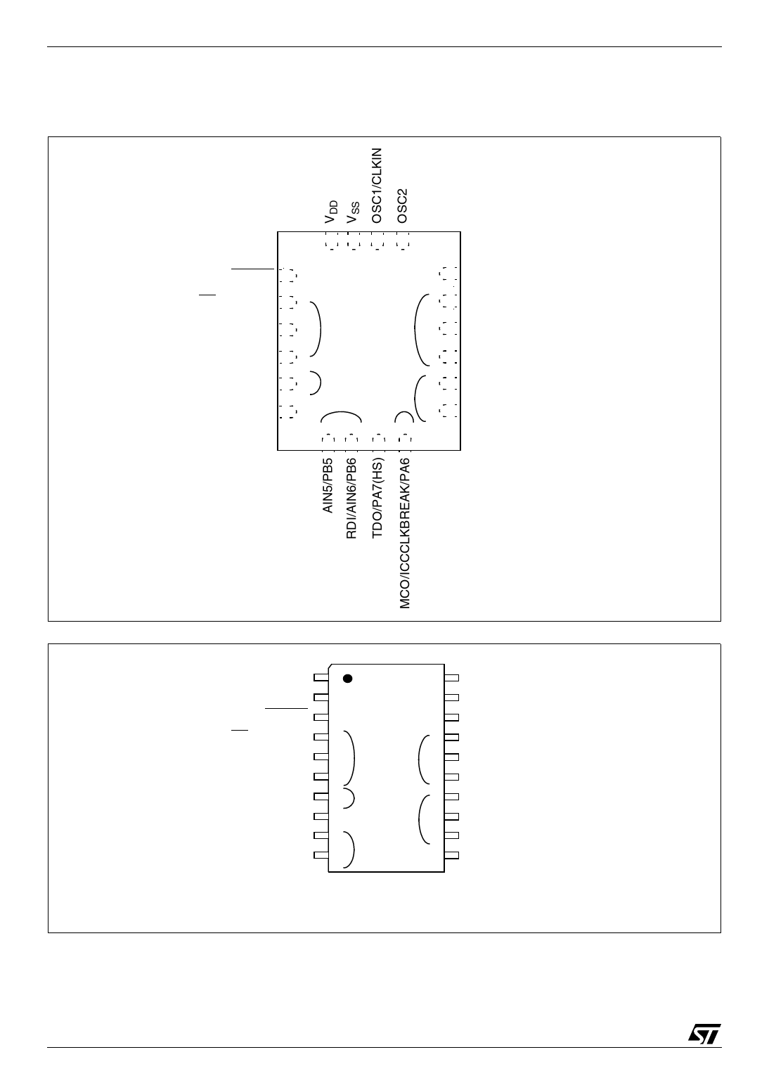
ST7LITE3
PIN DESCRIPTION (Cont’d)
Legend / Abbreviations for Table 1:
Type:
I = input, O = output, S = supply
In/Output level: CT= CMOS 0.3VDD/0.7VDD with input trigger
Output level: HS = 20mA high sink (on N-buffer only)
Port and control configuration:
– Input:
float = floating, wpu = weak pull-up, int = interrupt, ana = analog
– Output: OD = open drain, PP = push-pull
The RESET configuration of each pin is shown in bold which is valid as long as the device is in reset state.
Table 1. Device Pin Description
Pin
No.
Pin Name
Level
Port / Control
Main
Input
Output Function
(after
reset)
Alternate Function
1 VSS
S
2 VDD
S
3 RESET
I/O CT
X
4 PB0/AIN0/SS I/O CT
5 PB1/AIN1/SCK I/O CT
X
ei3
X
6 PB2/AIN2/MISO I/O CT X
7 PB3/AIN3/MOSI I/O CT X
8
PB4/AIN4/
CLKIN**
I/O CT X
9 PB5/AIN5
I/O CT X
10 PB6/AIN6/RDI I/O CT X
11 PA7/TDO
I/O CT HS X
ei2
X
ei2
X
Ground
Main power supply
X
Top priority non maskable interrupt (active low)
ADC Analog Input 0 or SPI Slave Select
(active low)
X X X Port B0 Caution: No negative current injection
allowed on this pin. For details, refer to
section 13.2.2 on page 130
ADC Analog Input 1 or SPI Serial Clock
X
X
X Port B1
Caution: No negative current injection
allowed on this pin. For details, refer to
section 13.2.2 on page 130
X
X
X Port B2
ADC Analog Input 2 or SPI Master In/
Slave Out Data
X
X
X Port B3
ADC Analog Input 3 or SPI Master Out
/ Slave In Data
X
X
X Port B4
ADC Analog Input 4 or External clock
input
X X X Port B5 ADC Analog Input 5
X X X Port B6 ADC Analog Input 6 or LINSCI Input
X X Port A7 LINSCI Output
6/167
1
Share Link: