AT89C5130A-PUTUM(2008) View Datasheet(PDF) - Atmel Corporation
Part Name
Description
Manufacturer
AT89C5130A-PUTUM Datasheet PDF : 188 Pages
| |||
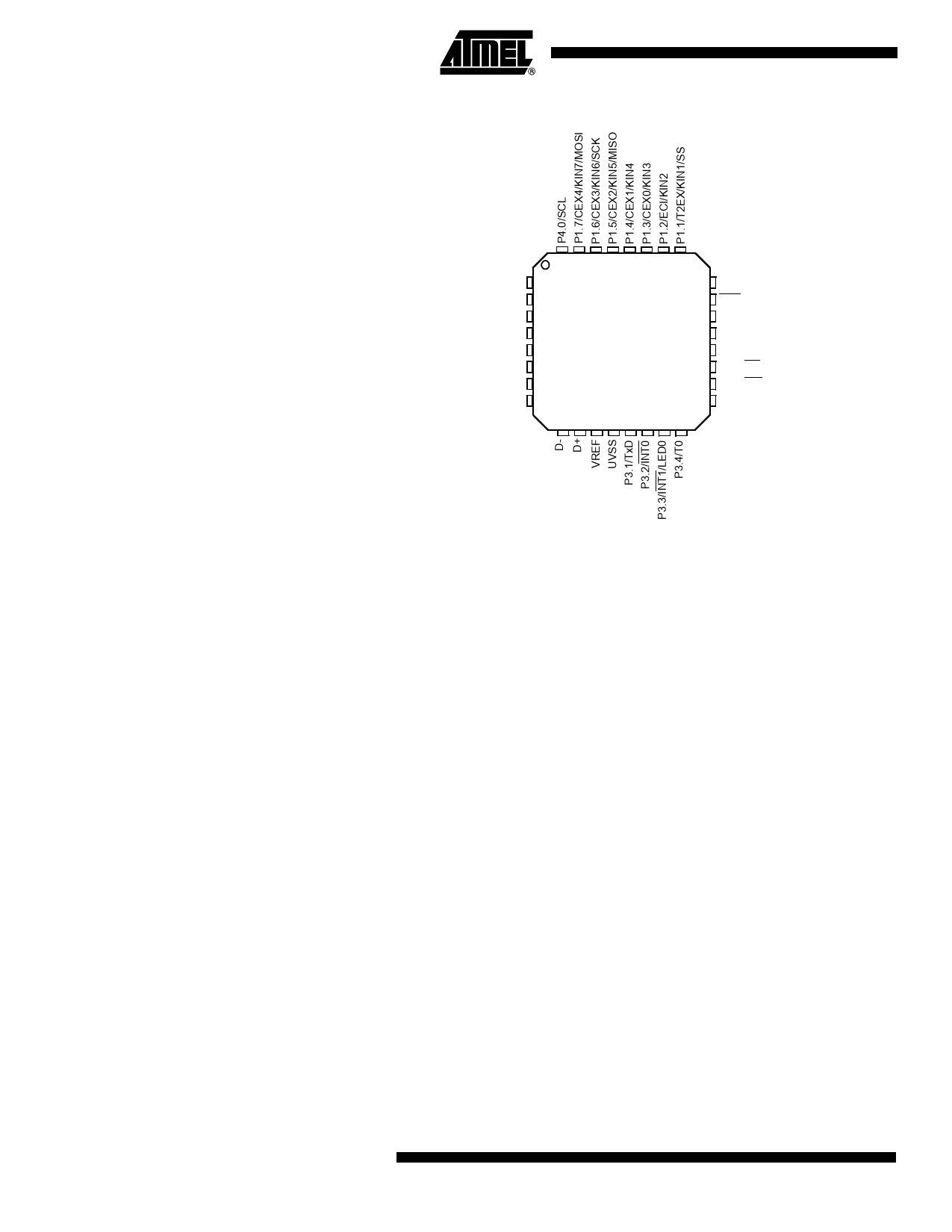
Figure 3-3. AT89C5130A/31A-M 32-pin QFN Pinout
32 31 30 29 28 27 26 25
P4.1/SDA 1
XTAL2 2
XTAL1 3
24 P1.0/T2/KIN0
23 RST
22 NC
VDD 4
UCAP 5
QFN32
21 VSS
20 NC
AVSS 6
19 P3.7/RD/LED3
P3.0/RxD 7
18 P3.6/WR/LED2
PLLF 8
17 P3.5/T1/LED1
9 10 11 12 13 14 15 16
Note : The metal plate can be connected to Vss
3.2 Signals
All the AT89C5130A/31A-M signals are detailed by functionality on Table 3-1 through Table 3-
12.
Table 3-1. Keypad Interface Signal Description
Signal
Name Type Description
KIN[7:0)
Keypad Input Lines
I Holding one of these pins high or low for 24 oscillator periods triggers a
keypad interrupt if enabled. Held line is reported in the KBCON register.
Alternate
Function
P1[7:0]
Table 3-2. Programmable Counter Array Signal Description
Signal
Name
ECI
Type Description
I External Clock Input
Alternate
Function
P1.2
6 AT89C5130A/31A-M
4337K–USB–04/08
Share Link: 