AT89C5131A-M(2005) View Datasheet(PDF) - Atmel Corporation
Part Name
Description
Manufacturer
AT89C5131A-M Datasheet PDF : 184 Pages
| |||
4337C–USB–02/05
AT89C5130A/31A-M
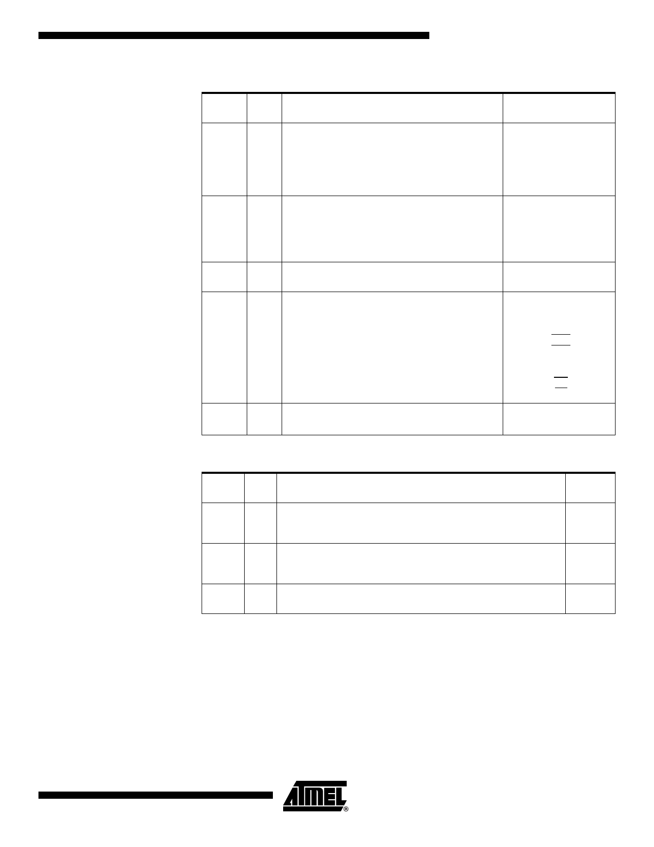
Table 8. Ports Signal Description
Signal
Name
P0[7:0]
Type Description
Port 0
P0 is an 8-bit open-drain bidirectional I/O port. Port 0
I/O
pins that have 1s written to them float and can be used
as high impedance inputs. To avoid any parasitic current
consumption, Floating P0 inputs must be pulled to VDD or
VSS.
P1[7:0]
I/O
Port 1
P1 is an 8-bit bidirectional I/O port with internal pull-ups.
P2[7:0]
I/O
Port 2
P2 is an 8-bit bidirectional I/O port with internal pull-ups.
P3[7:0]
I/O
Port 3
P3 is an 8-bit bidirectional I/O port with internal pull-ups.
P4[1:0]
I/O
Port 4
P4 is an 2-bit open drain port.
Alternate Function
AD[7:0]
KIN[7:0]
T2
T2EX
ECI
CEX[4:0]
A[15:8]
LED[3:0]
RxD
TxD
INT0
INT1
T0
T1
WR
RD
SCL
SDA
Table 9. Clock Signal Description
Signal
Name Type Description
Alternate
Function
Input to the on-chip inverting oscillator amplifier
XTAL1
I To use the internal oscillator, a crystal/resonator circuit is connected to this
-
pin. If an external oscillator is used, its output is connected to this pin.
Output of the on-chip inverting oscillator amplifier
XTAL2 O To use the internal oscillator, a crystal/resonator circuit is connected to this
-
pin. If an external oscillator is used, leave XTAL2 unconnected.
PLLF
I
PLL Low Pass Filter input
Receive the RC network of the PLL low pass filter.
-
Table 10. USB Signal Description
Signal
Name
D+
Type Description
I/O USB Data + signal
D-
VREF
I/O USB Data - signal
O
USB Reference Voltage
Connect this pin to D+ using a 1.5 kΩ resistor to use the Detach function.
Alternate
Function
-
-
-
9
Share Link: 