AT89C5131A-S3SUM View Datasheet(PDF) - Atmel Corporation
Part Name
Description
Manufacturer
AT89C5131A-S3SUM Datasheet PDF : 186 Pages
| |||
Signals
AT89C5130A/31A-M
All the AT89C5130A/31A-M signals are detailed by functionality on Table 1 through
Table 12.
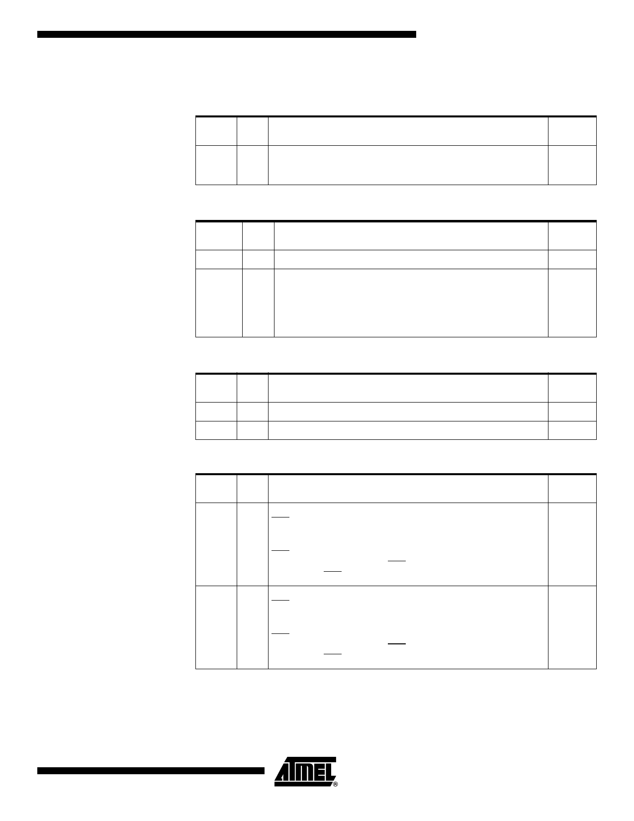
Table 1. Keypad Interface Signal Description
Signal
Name Type Description
KIN[7:0)
Keypad Input Lines
I Holding one of these pins high or low for 24 oscillator periods triggers a
keypad interrupt if enabled. Held line is reported in the KBCON register.
Alternate
Function
P1[7:0]
Table 2. Programmable Counter Array Signal Description
Signal
Name
ECI
Type Description
I External Clock Input
CEX[4:0]
Capture External Input
I/O
Compare External Output
Alternate
Function
P1.2
P1.3
P1.4
P1.5
P1.6
P1.7
Table 3. Serial I/O Signal Description
Signal
Name
RxD
TxD
Type Description
I Serial Input Port
O Serial Output Port
Alternate
Function
P3.0
P3.1
Table 4. Timer 0, Timer 1 and Timer 2 Signal Description
Signal
Name Type Description
Alternate
Function
INT0
Timer 0 Gate Input
INT0 serves as external run control for timer 0, when selected by GATE0
bit in TCON register.
I External Interrupt 0
INT0 input set IE0 in the TCON register. If bit IT0 in this register is set, bits
IE0 are set by a falling edge on INT0. If bit IT0 is cleared, bits IE0 is set by
a low level on INT0.
P3.2
INT1
Timer 1 Gate Input
INT1 serves as external run control for Timer 1, when selected by GATE1
bit in TCON register.
I External Interrupt 1
INT1 input set IE1 in the TCON register. If bit IT1 in this register is set, bits
IE1 are set by a falling edge on INT1. If bit IT1 is cleared, bits IE1 is set by
a low level on INT1.
P3.3
7
4337G–USB–11/06
Share Link: 