KAD2710L-27 View Datasheet(PDF) - Intersil
Part Name
Description
Manufacturer
KAD2710L-27 Datasheet PDF : 16 Pages
| |||
KAD2710L
Absolute Maximum Ratings
AVDD2 to AVSS. . . . . . . . . . . . . . . . . . . . . . . . . . . . . . -0.4V to 2.1V
AVDD3 to AVSS. . . . . . . . . . . . . . . . . . . . . . . . . . . . . . -0.4V to 3.7V
OVDD2 to OVSS . . . . . . . . . . . . . . . . . . . . . . . . . . . . . -0.4V to 2.1V
Analog Inputs to AVSS. . . . . . . . . . . . . . . . . -0.4V to AVDD3 + 0.3V
Clock Inputs to AVSS. . . . . . . . . . . . . . . . . . -0.4V to AVDD2 + 0.3V
Logic Inputs to AVSS (VREFSEL, CLKDIV) -0.4V to AVDD3 + 0.3V
Logic Inputs to OVSS (RST, 2SC) . . . . . . . . -0.4V to OVDD2 + 0.3V
VREF to AVSS . . . . . . . . . . . . . . . . . . . . . . . -0.4V to AVDD3 + 0.3V
Analog Output Currents . . . . . . . . . . . . . . . . . . . . . . . . . . . . . . 10mA
Logic Output Currents . . . . . . . . . . . . . . . . . . . . . . . . . . . . . . . 10mA
LVDS Output Currents . . . . . . . . . . . . . . . . . . . . . . . . . . . . . . . 20mA
Thermal Information
Operating Temperature . . . . . . . . . . . . . . . . . . . . . . .-40°C to +85°C
Storage Temperature . . . . . . . . . . . . . . . . . . . . . . . .-65°C to +150°C
Junction Temperature . . . . . . . . . . . . . . . . . . . . . . . . . . . . . . +150°C
CAUTION: Do not operate at or near the maximum ratings listed for extended periods of time. Exposure to such conditions may adversely impact product reliability and
result in failures not covered by warranty.
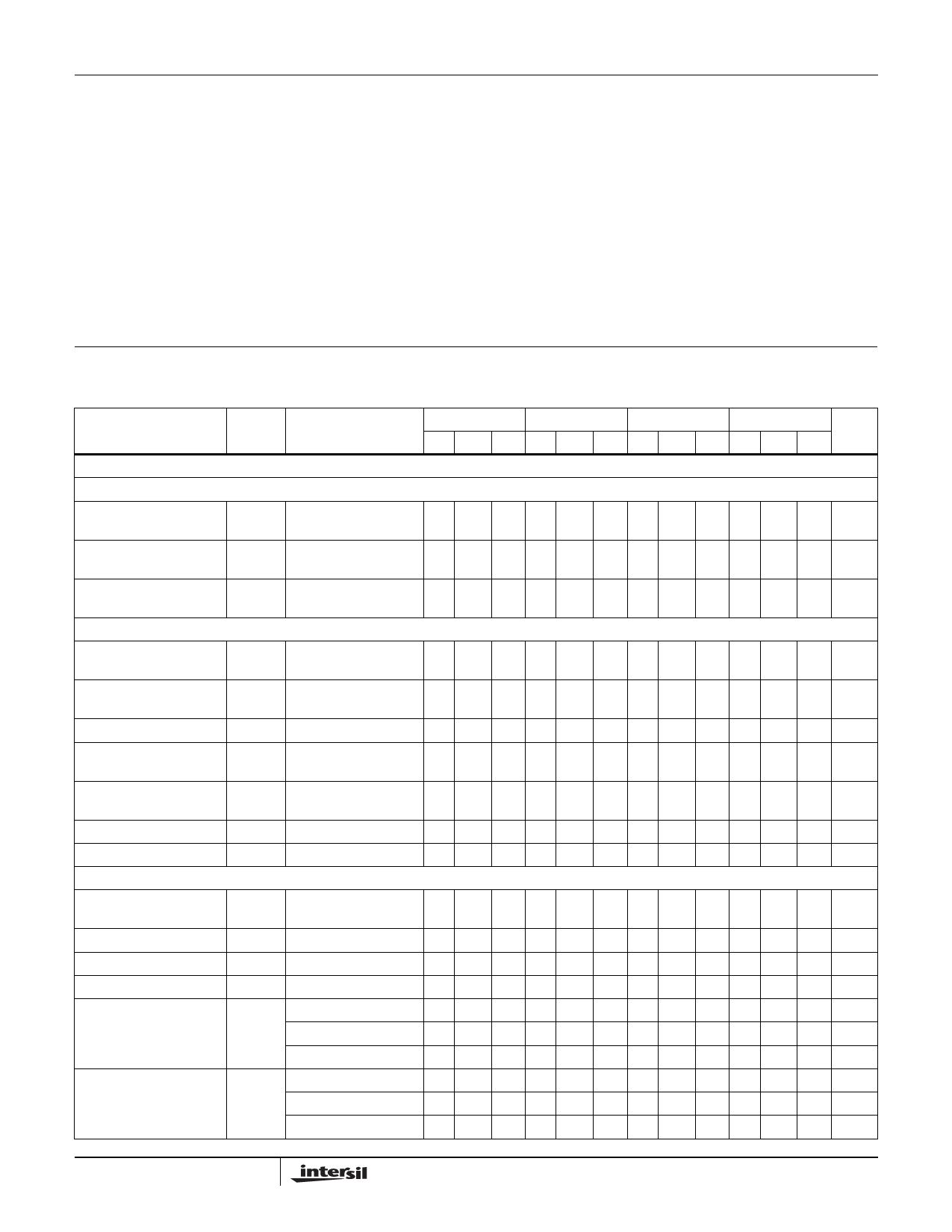
Electrical Specifications All specifications apply under the following conditions unless otherwise noted: AVDD2 = 1.8V, AVDD3 = 3.3V,
OVDD = 1.8V, TA = -40°C to +85°C (typical specifications at +25°C), fSAMPLE = 275MSPS, 210MSPS,
170MSPS and 105MSPS, fIN = Nyquist at -0.5dBFS.
KAD2710L-27 KAD2710L-21 KAD2710L-17 KAD2710L-10
PARAMETER
SYMBOL
CONDITIONS
MIN TYP MAX MIN TYP MAX MIN TYP MAX MIN TYP MAX UNITS
DC SPECIFICATIONS
Analog Input
Full-Scale Analog Input
VFS
Range
1.4 1.5 1.6 1.4 1.5 1.6 1.4 1.5 1.6 1.4 1.5 1.6 VP-P
Full Scale Range Temp.
Drift
AVTC Full Temp
230
210
198
178
ppm/°C
Common-Mode Output
Voltage
VCM
860
860
860
860
mV
Power Requirements
1.8V Analog Supply
Voltage
AVDD2
1.7 1.8 1.9 1.7 1.8 1.9 1.7 1.8 1.9 1.7 1.8 1.9 V
3.3V Analog Supply
Voltage
AVDD3
3.15 3.3 3.45 3.15 3.3 3.45 3.15 3.3 3.45 3.15 3.3 3.45 V
1.8V Digital Supply Voltage OVDD
1.7 1.8 1.9 1.7 1.8 1.9 1.7 1.8 1.9 1.7 1.8 1.9 V
1.8V Analog Supply
Current
IAVDD2
44 51
38 42
35 39
29 33 mA
3.3V Analog Supply
Current
IAVDD3
1.8V Digital Supply Current
I
OVDD
Power Dissipation
PD
AC SPECIFICATIONS
41 45
36 41
278 314
33 37
35 39
240 268
28 32
34 38
217 244
21 24 mA
31 35 mA
178 202 mW
Maximum Conversion
Rate
fS MAX
275
210
170
105
MSPS
Minimum Conversion Rate fS MIN
Differential Nonlinearity
DNL
50
50
50
50 MSPS
-1.0 ±0.8 1.5 -1.0 ±0.8 1.5 -1.0 ±0.8 1.5 -1.0 ±0.8 1.5 LSB
Integral Nonlinearity
INL
-2.5 ±1.0 2.0 -2.5 ±1.0 1.5 -2.5 ±1.0 1.5 -2.5 ±1.0 1.5 LSB
Signal-to-Noise Ratio
Signal-to-Noise and
Distortion
SNR fIN = 10MHz
fIN = Nyquist
fIN = 430MHz
SINAD fIN = 10MHz
fIN = Nyquist
fIN = 430MHz
55.7
53.5 55.6
55.2
55.3
52.5 55.2
54.4
56.4
53.5 56.2
54.8
56.1
52.5 56.0
53.7
56.6
53.5 56.5
54.6
56.3
52.5 56.2
53.4
56.6
53.5 56.5
54.5
56.3
52.5 56.2
53.2
dBFS
dBFS
dBFS
dBFS
dBFS
dBFS
4
FN6818.0
December 5, 2008
Share Link: 