ADM5170APZ View Datasheet(PDF) - Analog Devices
Part Name
Description
Manufacturer
ADM5170APZ Datasheet PDF : 7 Pages
| |||
ABSOLUTE MAXIMUM RATINGS*
(T =
A
25°C
unless
otherwise
noted)
VDD . . . . . . . . . . . . . . . . . . . . . . . . . . . . . . . . . . . . . . . . . . . +15 V
VSS . . . . . . . . . . . . . . . . . . . . . . . . . . . . . . . . . . . . . . . . . . . . . –15 V
Input Voltages
VIN . . . . . . . . . . . . . . . . . . . . . . . . . . . . . . . –0.3 to (VDD + 0.3 V)
Ouput Voltages
VOUT . . . . . . . . . . . . . . . . . . . . . . . . . . . . . . . . . . –12 V to +12 V
Output Short Circuit Duration . . . . . . . . . . . . . . . . . . Continuous
Power Dissipation PLCC . . . . . . . . . . . . . . . . . . . . . . . 1000 mW
(Derate at 10 mW/°C above +50°C)
θJA, Thermal Impedance . . . . . . . . . . . . . . . . . . . . . . . . . 80°C/W
Operating Temperature Range
Industrial (A Version) . . . . . . . . . . . . . . . . . . . . –40°C to +85°C
Lead Temperature (Soldering 10 sec) . . . . . . . . . . . . . . . . +300°C
Vapour Phase (60 sec) . . . . . . . . . . . . . . . . . . . . . . . . . . +215°C
Infrared (15 sec) . . . . . . . . . . . . . . . . . . . . . . . . . . . . . . . +220°C
*This is a stress rating only and functional operation of the device at these or any
other conditions above those indicated in the operation sections of this specifica-
tion is not implied. Exposure to absolute maximum rating conditions for extended
periods of time may affect reliability.
ADM5170
CAUTION
ESD (electrostatic discharge) sensitive device. Electrostatic charges as high as 4000 V readily
accumulate on the human body and test equipment and can discharge without detection. Although
the ADM5170 features proprietary ESD protection circuitry, permanent damage may occur on
devices subjected to high energy electrostatic discharges. Therefore, proper ESD precautions are
recommended to avoid performance degradation or loss of functionality.
WARNING!
ESD SENSITIVE DEVICE
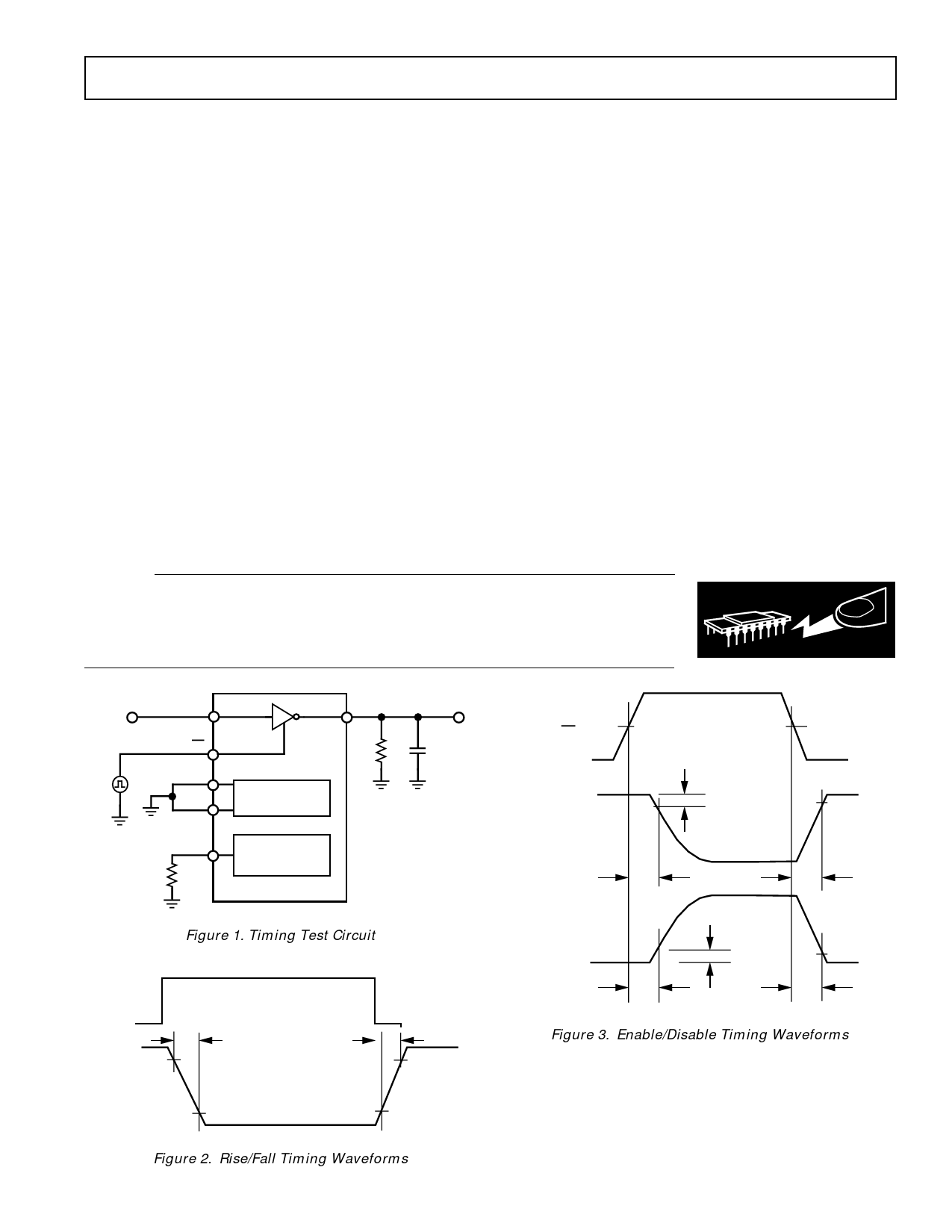
VIN
EN
MS+
MS–
SRA
RS-232/RS-423
MODE SELECT
SLEW RATE
CONTROL
RL
CL
Figure 1. Timing Test Circuit
VIN
tF
10%
VOUT
90%
tR
90%
10%
Figure 2. Rise/Fall Timing Waveforms
INPUT
EN
1.5V
VOH
OUTPUT
VIN = 0V
0.5V
1.5V
90%
OUTPUT
VIN = 5V
VOL
tHZ
0.5V
tLZ
tZH
90%
tZL
Figure 3. Enable/Disable Timing Waveforms
REV. A
–3–
Share Link: 