SST25VF032B-66-4I-QAE View Datasheet(PDF) - Microchip Technology
Part Name
Description
Manufacturer
SST25VF032B-66-4I-QAE Datasheet PDF : 33 Pages
| |||
A Microchip Technology Company
32 Mbit SPI Serial Flash
SST25VF032B
Instructions
Data Sheet
Instructions are used to read, write (Erase and Program), and configure the SST25VF032B. The
instruction bus cycles are 8 bits each for commands (Op Code), data, and addresses. The Write-
Enable (WREN) instruction must be executed prior any Byte-Program, Auto Address Increment (AAI)
programming, Sector-Erase, Block-Erase, Write-Status-Register, or Chip-Erase instructions. The com-
plete list of instructions is provided in Table 5.
All instructions are synchronized off a high to low transition of CE#. Inputs will be accepted on the ris-
ing edge of SCK starting with the most significant bit. CE# must be driven low before an instruction is
entered and must be driven high after the last bit of the instruction has been shifted in (except for
Read, Read-ID, and Read-Status-Register instructions). Any low to high transition on CE#, before
receiving the last bit of an instruction bus cycle, will terminate the instruction in progress and return the
device to standby mode. Instruction commands (Op Code), addresses, and data are all input from the
most significant bit (MSB) first.
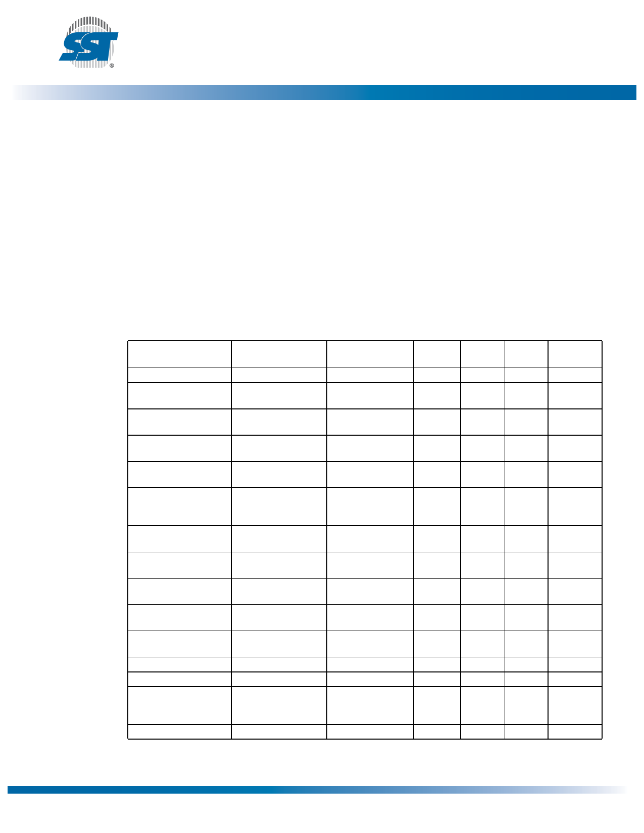
Table 5: Device Operation Instructions (1 of 2)
Instruction
Description
Address Dummy Data Maximum
Op Code Cycle1 Cycle(s)2 Cycle(s) Cycle(s) Frequency
Read
Read Memory
0000 0011b (03H)
3
0
1 to 25 MHz
High-Speed Read
Read Memory at
higher speed
0000 1011b (0BH)
3
1
1 to 80 MHz
4 KByte Sector-Erase3 Erase 4 KByte of
0010 0000b (20H)
3
0
0
80 MHz
memory array
32 KByte Block-Erase4 Erase 32KByte block 0101 0010b (52H)
3
0
0
80 MHz
of memory array
64 KByte Block-Erase5 Erase 64 KByte block 1101 1000b (D8H)
3
0
0
80 MHz
of memory array
Chip-Erase
Erase Full Memory 0110 0000b (60H)
0
Array
or
1100 0111b (C7H)
0
0
80 MHz
Byte-Program
To Program One
0000 0010b (02H)
3
Data Byte
0
1
80 MHz
AAI-Word-Program6 Auto Address Incre- 1010 1101b (ADH)
3
ment Programming
0
2 to 80 MHz
RDSR7
Read-Status-Regis- 0000 0101b (05H)
0
ter
0
1 to 80 MHz
EWSR
Enable-Write-Status- 0101 0000b (50H)
0
Register
0
0
80 MHz
WRSR
Write-Status-Regis- 0000 0001b (01H)
0
ter
0
1
80 MHz
WREN
Write-Enable
0000 0110b (06H)
0
0
0
80 MHz
WRDI
Write-Disable
0000 0100b (04H)
0
0
0
80 MHz
RDID8
Read-ID
1001 0000b (90H)
3
or
1010 1011b (ABH)
0
1 to 80 MHz
JEDEC-ID
JEDEC ID read
1001 1111b (9FH)
0
0
3 to 80 MHz
©2011 Silicon Storage Technology, Inc.
9
DS25071A
12/11
Share Link: 