IRS21867S View Datasheet(PDF) - International Rectifier
Part Name
Description
Manufacturer
IRS21867S Datasheet PDF : 21 Pages
| |||
IRS21867S
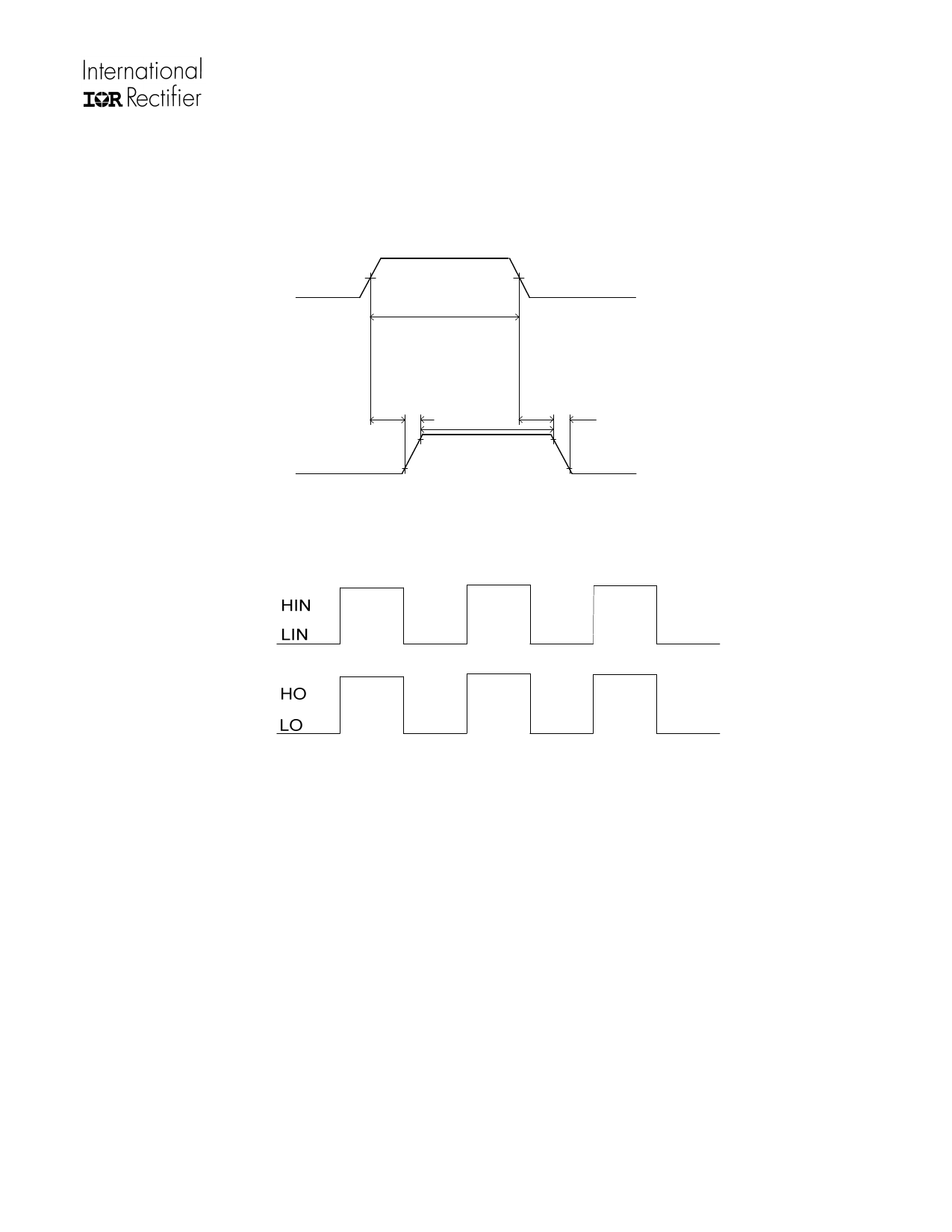
Switching and Timing Relationships
The relationships between the input and output signals of the IRS21867 are illustrated below in Figures 3, 4. From
these figures, we can see the definitions of several timing parameters (i.e., PWIN, PWOUT, tON, tOFF, tR, and tF)
associated with this device.
LINx
(or HINx) 50%
50%
PWIN
LOx
(or HOx)
tON tR
90%
10%
PWOUT
tOFF tF
90%
10%
Figure 3: Switching time waveforms
Figure 4: Input/output timing diagram
Matched Propagation Delays
The IRS21867 is designed with propagation delay matching circuitry. With this feature, the IC’s response at the
output to a signal at the input requires approximately the same time duration (i.e., tON, tOFF) for both the low-side
channels and the high-side channels; the maximum difference is specified by the delay matching parameter (MT).
The propagation turn-on delay (tON) is matched to the propagation turn-on delay (tOFF).
www.irf.com
© 2010 International Rectifier
10
Share Link: 