LH28F016SC-L View Datasheet(PDF) - Sharp Electronics
Part Name
Description
Manufacturer
LH28F016SC-L Datasheet PDF : 44 Pages
| |||
LH28F016SC-L/SCH-L
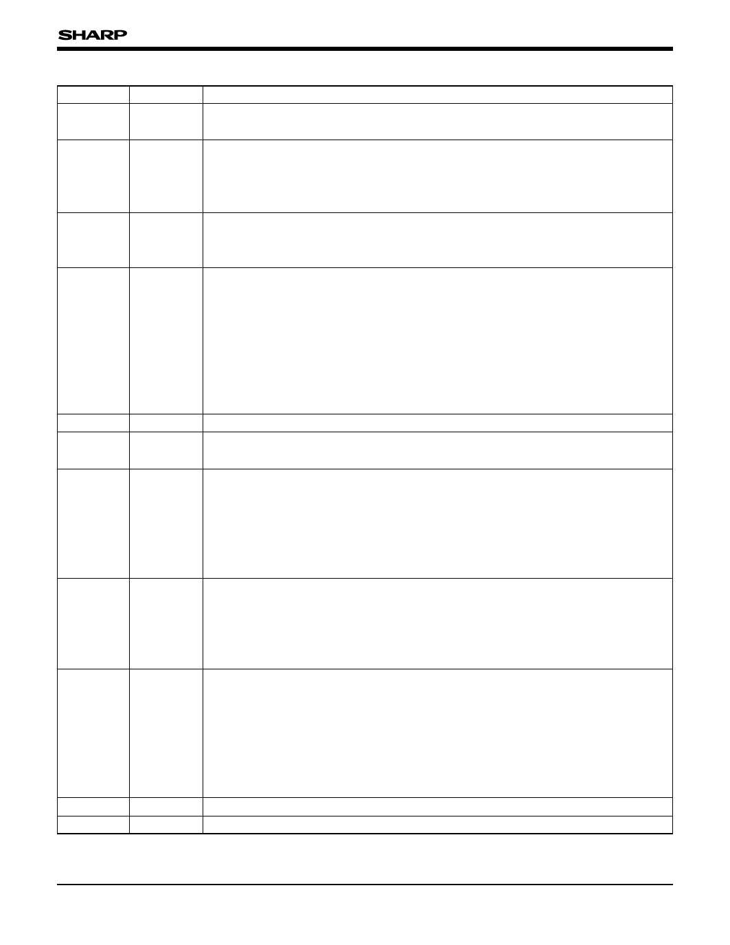
PIN DESCRIPTION
SYMBOL
TYPE
A0-A20
INPUT
DQ0-DQ7
INPUT/
OUTPUT
CE#
INPUT
RP#
INPUT
OE#
WE#
INPUT
INPUT
RY/BY# OUTPUT
VPP
SUPPLY
VCC
SUPPLY
GND
NC
SUPPLY
NAME AND FUNCTION
ADDRESS INPUTS : Inputs for addresses during read and write operations. Addresses
are internally latched during a write cycle.
DATA INPUT/OUTPUTS : Inputs data and commands during CUI write cycles; outputs
data during memory array, status register, and identifier code read cycles. Data pins
float to high-impedance when the chip is deselected or outputs are disabled. Data is
internally latched during a write cycle.
CHIP ENABLE : Activates the device's control logic, input buffers, decoders, and sense
amplifiers. CE#-high deselects the device and reduces power consumption to standby
levels.
RESET/DEEP POWER-DOWN : Puts the device in deep power-down mode and resets
internal automation. RP#-high enables normal operation. When driven low, RP# inhibits
write operations which provide data protection during power transitions. Exit from deep
power-down sets the device to read array mode. RP# at VHH enables setting of the
master lock-bit and enables configuration of block lock-bits when the master lock-bit is
set. RP# = VHH overrides block lock-bits thereby enabling block erase and byte write
operations to locked memory blocks. Block erase, byte write, or lock-bit configuration
with VIH < RP# < VHH produce spurious results and should not be attempted.
OUTPUT ENABLE : Gates the device's outputs during a read cycle.
WRITE ENABLE : Controls writes to the CUI and array blocks. Addresses and data are
latched on the rising edge of the WE# pulse.
READY/BUSY : Indicates the status of the internal WSM. When low, the WSM is
performing an internal operation (block erase, byte write, or lock-bit configuration).
RY/BY#-high indicates that the WSM is ready for new commands, block erase is
suspended, and byte write is inactive, byte write is suspended, or the device is in deep
power-down mode. RY/BY# is always active and does not float when the chip is
deselected or data outputs are disabled.
BLOCK ERASE, BYTE WRITE, LOCK-BIT CONFIGURATION POWER SUPPLY : For
erasing array blocks, writing bytes, or configuring lock-bits. With VPP ≤ VPPLK, memory
contents cannot be altered. Block erase, byte write, and lock-bit configuration with an
invalid VPP (see Section 6.2.3 "DC CHARACTERISTICS") produce spurious results
and should not be attempted.
DEVICE POWER SUPPLY : Internal detection configures the device for 2.7 V , 3.3 V or
5 V operation. To switch from one voltage to another, ramp VCC down to GND and then
ramp VCC to the new voltage. Do not float any power pins. With VCC ≤ VLKO, all write
attempts to the flash memory are inhibited. Device operations at invalid VCC voltage
(see Section 6.2.3 "DC CHARACTERISTICS") produce spurious results and should
not be attempted. Block erase, byte write and lock-bit configuration operations with VCC
< 3.0 V are not supported.
GROUND : Do not float any ground pins.
NO CONNECT : Lead is not internal connected; recommend to be floated.
-4-
Share Link: 