MIC29302A View Datasheet(PDF) - Micrel
Part Name
Description
Manufacturer
MIC29302A Datasheet PDF : 18 Pages
| |||
Micrel, Inc.
MIC29302A
Absolute Maximum Ratings(1)
Input Supply Voltage (VIN)(1) ........................... –20V to +20V
Enable Input Voltage (VEN)................................ –0.3V to VIN
Lead Temperature (soldering, 5 sec.) ........................ 260°C
Power Dissipation ..................................... Internally Limited
Storage Temperature Range .................... –65°C to +150°C
ESD Rating all pins(3)
Operating Ratings(2)
Operating Junction Temperature .............. −40°C to +125°C
Operating Input Voltage ....................................... 3V to 16V
Package Thermal Resistance
TO-263 (θJC).........................................................3°C/W
TO-252 (θJC).........................................................3°C/W
TO-252 (θJA) ...................................................... 35°C/W
TO-263 (θJA).......................................................28°C/W
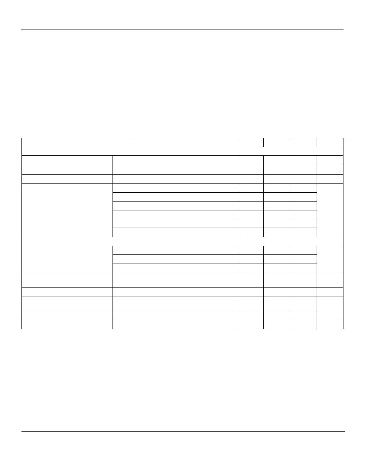
Electrical Characteristics(4)
VIN = 4.2V; IOUT = 100mA; TA = 25°C, bold values indicate −40°C≤ TJ ≤ +125°C, unless noted.
Parameter
Condition
Min.
Typ.
Max.
Units
Output Voltage
Output Voltage Accuracy(5)
100mA ≤ IOUT ≤3A, (VOUT + 1V) ≤ VIN ≤ 16V
−2
2
%
Line Regulation
IOUT = 100mA, (VOUT + 1V) ≤ VIN ≤ 16V
0.1
0.5
%
Load Regulation
VIN = VOUT + 1V, 100mA ≤ IOUT ≤ 3A
0.2
1
%
IOUT = 100mA
80
200
IOUT = 750mA
220
Dropout Voltage(6)
Ground Current
IOUT = 1.5A
IOUT = 2.0A
IOUT = 2.5A
IOUT = 3A
275
mV
375
630
430
720
450
800
IOUT = 750mA, VIN = VOUT + 1V
5
20
Ground Current
IOUT = 1.5A
15
mA
IOUT = 3A
60
150
IGRNDDO Ground Pin Current
@ Dropout
VIN = 0.5V less than specified VOUT × IOUT = 10mA
2
Current Limit
VOUT = 0V(7)
3
4
A
en, Output Noise Voltage
(10Hz to 100kHz
IL = 100mA
Ground Pin Current in Shutdown
CL = 10µF
CL = 33µF
Input Voltage VIN = 16V
400
µVRMS
260
32
µA
Notes:
1. Exceeding the absolute maximum rating may damage the device.
2. The device is not guaranteed to function outside its operating rating.
3. Devices are ESD sensitive. Handling precautions recommended. Human body model, 1.5kΩ in series with 100pF.
4. Specification for packaged product only
5. Output voltage temperature coefficient is defined as the worst case voltage change divided by the total temperature change.
6. Dropout voltage is defined as the input-to-output differential when output voltage drops to 99% of its normal value with VOUT + 1V applied to VIN.
7. VIN =VOUT (nominal) + 1V. For example, use VIN = 4.3V for a 3.3V regulator or use 6V for a 5V regulator. Employ pulse testing procedure for current limit.
October 3, 2014
3
Revision 2.0
Share Link: 