PIC16F1503 View Datasheet(PDF) - Microchip Technology
Part Name
Description
Manufacturer
PIC16F1503 Datasheet PDF : 352 Pages
| |||
PIC16(L)F1503
3.3 Data Memory Organization
The data memory is partitioned in 32 memory banks
with 128 bytes in a bank. Each bank consists of
(Figure 3-2):
• 12 core registers
• 20 Special Function Registers (SFR)
• Up to 80 bytes of General Purpose RAM (GPR)
• 16 bytes of common RAM
The active bank is selected by writing the bank number
into the Bank Select Register (BSR). Unimplemented
memory will read as ‘0’. All data memory can be
accessed either directly (via instructions that use the
file registers) or indirectly via the two File Select
Registers (FSR). See Section 3.6 “Indirect
Addressing” for more information.
Data memory uses a 12-bit address. The upper five bits
of the address define the Bank address and the lower
seven bits select the registers/RAM in that bank.
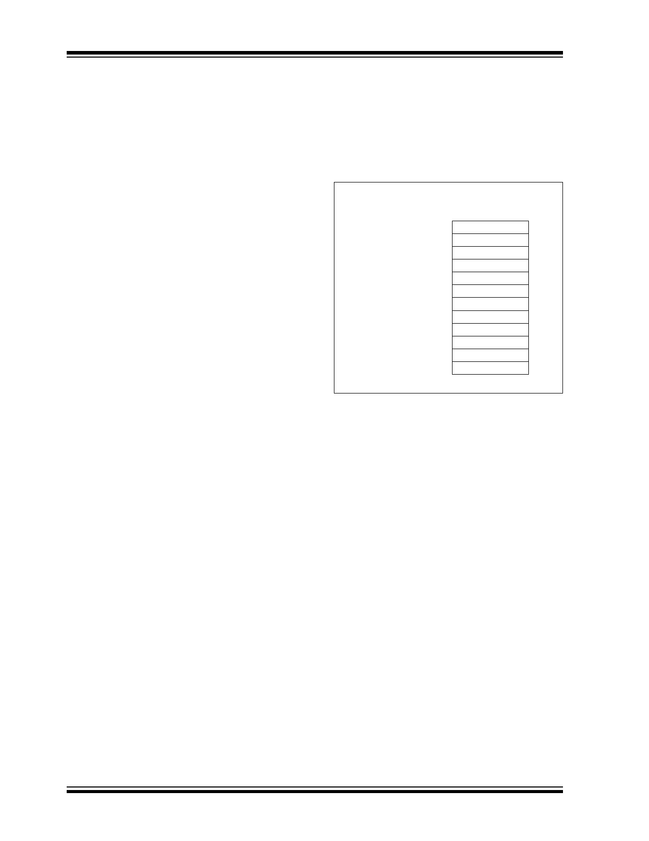
3.3.1 CORE REGISTERS
The core registers contain the registers that directly
affect the basic operation. The core registers occupy
the first 12 addresses of every data memory bank
(addresses x00h/x08h through x0Bh/x8Bh). These
registers are listed below in Table 3-2. For detailed
information, see Table 3-4.
TABLE 3-2: CORE REGISTERS
Addresses
x00h or x80h
x01h or x81h
x02h or x82h
x03h or x83h
x04h or x84h
x05h or x85h
x06h or x86h
x07h or x87h
x08h or x88h
x09h or x89h
x0Ah or x8Ah
x0Bh or x8Bh
BANKx
INDF0
INDF1
PCL
STATUS
FSR0L
FSR0H
FSR1L
FSR1H
BSR
WREG
PCLATH
INTCON
DS40001607D-page 16
2011-2015 Microchip Technology Inc.
Share Link: 