H5TQ2G43CFR-XXC View Datasheet(PDF) - Hynix Semiconductor
Part Name
Description
Manufacturer
H5TQ2G43CFR-XXC Datasheet PDF : 33 Pages
| |||
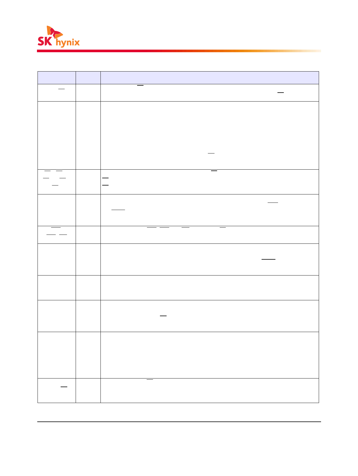
Pin Functional Description
Symbol
CK, CK
CKE, (CKE0),
(CKE1)
CS, (CS0),
(CS1), (CS2),
(CS3)
ODT, (ODT0),
(ODT1)
RAS.
CAS. WE
DM, (DMU),
(DML)
BA0 - BA2
A0 - A15
A10 / AP
A12 / BC
Type
Input
Input
Input
Input
Input
Function
Clock: CK and CK are differential clock inputs. All address and control input signals are
sampled on the crossing of the positive edge of CK and negative edge of CK.
Clock Enable: CKE HIGH activates, and CKE Low deactivates, internal clock signals and
device input buffers and output drivers. Taking CKE Low provides Precharge Power-Down
and Self-Refresh operation (all banks idle), or Active Power-Down (row Active in any
bank).
CKE is asynchronous for Self-Refresh exit. After VREFCA and VREFDQ have become stable
during the power on and initialization sequence, they must be maintained during all
operations (including Self-Refresh). CKE must be maintained high throughout read and
write accesses. Input buffers, excluding CK, CK, ODT and CKE, are disabled during power-
down. Input buffers, excluding CKE, are disabled during Self-Refresh.
Chip Select: All commands are masked when CS is registered HIGH.
CS provides for external Rank selection on systems with multiple Ranks.
CS is considered part of the command code.
On Die Termination: ODT (registered HIGH) enables termination resistance internal to the
DDR3 SDRAM. When enabled, ODT is only applied to each DQ, DQS, DQS and DM/TDQS,
NU/TDQS (When TDQS is enabled via Mode Register A11=1 in MR1) signal for x4/x8
configurations.
Command Inputs: RAS, CAS and WE (along with CS) define the command being entered.
Input
Input
Input
Input
Input
Input Data Mask: DM is an input mask signal for write data. Input data is masked when
DM is sampled HIGH coincident with that input data during a Write access. DM is sampled
on both edges of DQS. For x8 device, the function of DM or TDQS/TDQS is enabled by
Mode Register A11 setting in MR1.
Bank Address Inputs: BA0 - BA2 define to which bank an Active, Read, Write or Precharge
command is being applied. Bank address also determines if the mode register or extended
mode register is to be accessed during a MRS cycle.
Address Inputs: Provide the row address for Active commands and the column address for
Read/Write commands to select one location out of the memory array in the respective
bank. (A10/AP and A12/BC have additional functions, see below).
The address inputs also provide the op-code during Mode Register Set commands.
Auto-precharge: A10 is sampled during Read/Write commands to determine whether
Autoprecharge should be performed to the accessed bank after the Read/Write operation.
(HIGH: Autoprecharge; LOW: no Autoprecharge).A10 is sampled during a Precharge
command to determine whether the Precharge applies to one bank (A10 LOW) or all
banks (A10 HIGH). If only one bank is to be precharged, the bank is selected by bank
addresses.
Burst Chop: A12 / BC is sampled during Read and Write commands to determine if burst
chop (on-the-fly) will be performed.
(HIGH, no burst chop; LOW: burst chopped). See command truth table for details.
Rev. 1.0 / Apr. 2013
7
Share Link: 