MC34271FB View Datasheet(PDF) - ON Semiconductor
Part Name
Description
Manufacturer
MC34271FB Datasheet PDF : 12 Pages
| |||
MC34271
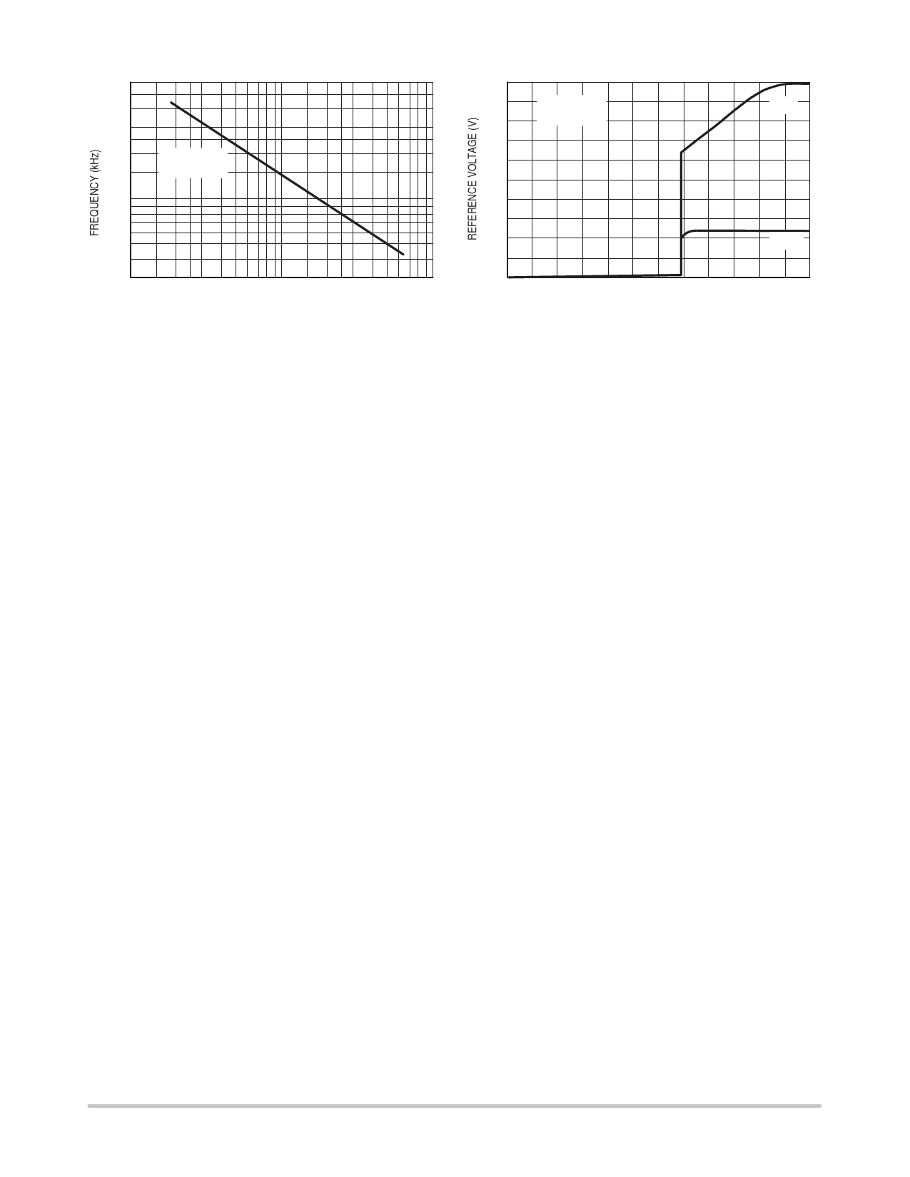
1000
5.0
RT = 169 k
VA
4.0
TA = 25°C
VDD = 6.0 V
3.0
TA = 25°C
100
2.0
1.0
Vref
10
0
100
1000
TIMING RESISTANCE (kΩ, s)
Figure 9. Frequency versus Timing
0
0
1.0
2.0
3.0
4.0
5.0
6.0
VDD LEVEL (V)
Figure 10. VA, Vref versus VDD
OPERATING DESCRIPTION
The MC34271 is a monolithic, fixed frequency power
switching regulator specifically designed for dc to dc
converter and battery powered applications. This device
operates as a fixed frequency, voltage mode regulator
containing all the active functions required to directly
implement step–up, step–down and voltage inverting
converters with a minimum number of external components.
Potential markets include battery powered, handheld,
automotive, computer, industrial and cost sensitive
consumer products. A description of each section is given
below with the representative block diagram shown in
Figure 11.
Oscillator
The oscillator frequency is programmed by resistor RT.
The charge to discharge ratio is controlled to yield a 95%
maximum duty cycle at the switch outputs. During the fall
time of the internal sawtooth waveform, the oscillator
generates an internal blanking pulse that holds the inverting
input of the AND gates high, disabling the output switching
MOSFETs. The internal sawtooth waveform has a nominal
peak voltage of 3.3 V and a valley voltage of 1.7 V.
Pulse Width Modulators
Both pulse width modulators consist of a comparator with
the oscillator ramp voltage applied to the noninverting input,
while the error amplifier output is applied to the inverting
input. A third input to the comparator has a 0.5 mA typical
current source that can be used to implement soft start.
Output switch conduction is initiated when the ramp
waveform is discharged to the valley voltage. As the ramp
voltage increases to a voltage that exceeds the error
amplifier output, the latch resets, terminating output
MOSFET conduction for the duration of the oscillator ramp.
This PWM/latch combination prevents multiple output
pulses during a given oscillator cycle.
Each PWM circuit is enabled by a logic input. When
disabled, the entire block is turned off, drawing only leakage
current from the power source. Shared circuits, like the
reference and oscillator, can be activated by either EN1
or EN2.
Circuit #1 has an ELD output which may be used to drive
an LCD or backlight. Its output frequency is the oscillator
frequency divided by 1024.
Error Amplifiers and Reference
Each error amplifier is provided with access to both
inverting and noninverting inputs, and the output. The Error
Amplifiers’ Common Mode Input Range is 0 to 2.5 V. The
amplifiers have a minimum dc voltage gain of 60 dB. The
1.25 V reference has an accuracy of ± 4.0% at room
temperature.
External loop compensation is required for converter
stability. A simple low–pass filter is formed by connecting
a resistive divider from the output to the error amplifier
inverting input, and a series resistor–capacitor from the error
amplifier output also to the to the inverting input. The step
down converter is easiest to compensate for stability. The
step–up and voltage inverting configurations, when
operated as continuous conduction boost or flyback
converters, are more difficult to compensate, and may
require a lower loop design bandwidth.
MOSFET Switch Outputs
The output MOSFETs are designed to switch a maximum
of 60 V, with a peak drain current capability of 500 mA. In
circuit #1 an additional DRV1 output is provided for
interfacing with an external MOSFET.The gates of the
MOSFETs are held low when the circuit is disabled.
Auxiliary Output Voltages
Output voltages V0 through V4 are provided for use as
references or bias voltages. V0 is the circuit #2 output
voltage, when an internal FET switch is activated. The other
auxiliary output voltages are proportional to VB. The
amplifiers for V1 and V2 are powered from V0, while the
amplifiers for V3 and V4 are powered from VDD.
http://onsemi.com
6
Share Link: 