NT5CB128M8DN View Datasheet(PDF) - Nanya Technology
Part Name
Description
Manufacturer
NT5CB128M8DN Datasheet PDF : 138 Pages
| |||
NT5CB128M8DN/NT5CB64M16DP
NT5CC128M8DN/NT5CC64M16DP
1Gb DDR3 D-die SDRAM
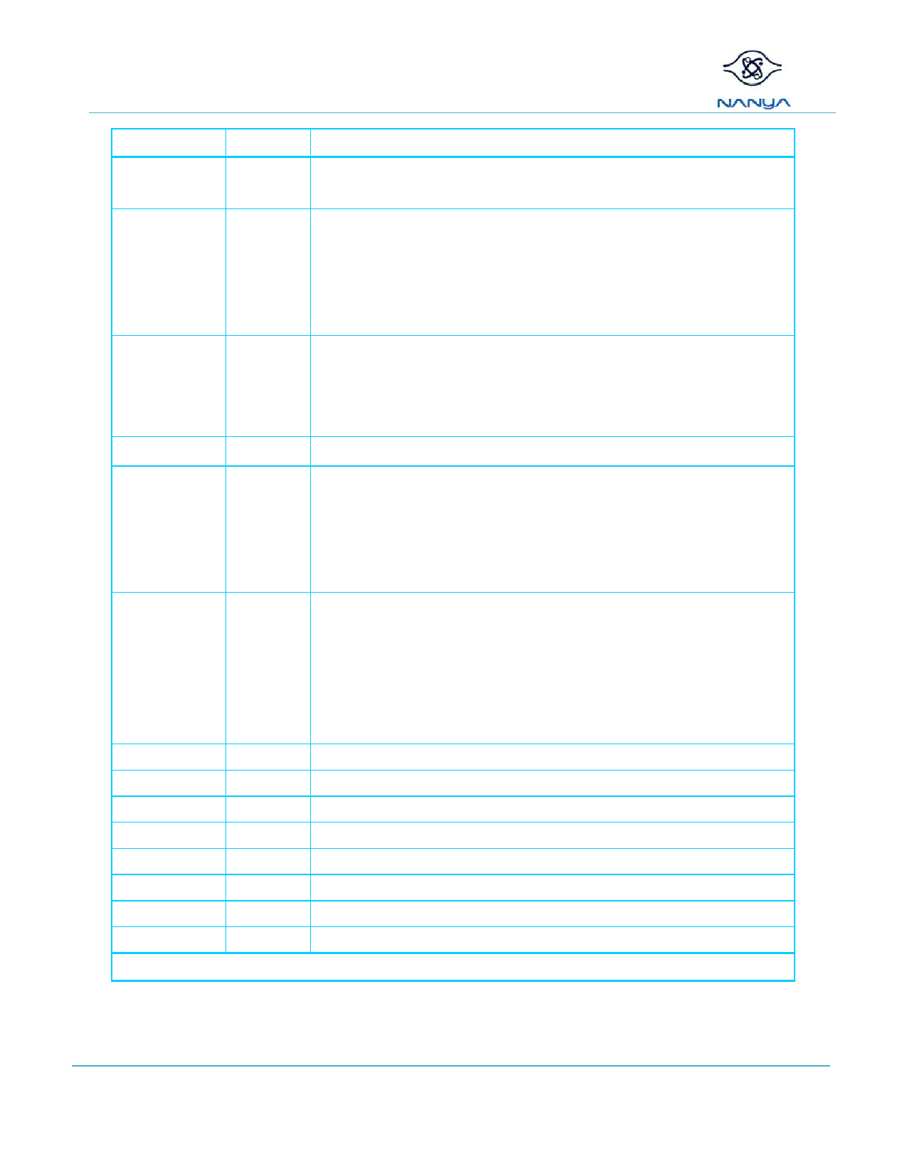
Symbol
Type
Function
A12/
ODT, (ODT0),
(ODT1)
Input
Input
Burst Chop: A12/ is sampled during Read and Write commands to determine if
burst chop (on the fly) will be performed. (HIGH - no burst chop; LOW - burst chopped).
On Die Termination: ODT (registered HIGH) enables termination resistance internal
to the DDR3/L SDRAM. When enabled, ODT is applied to each DQ, DQS, and
DM/TDQS, NU/
(when TDQS is enabled via Mode Register A11=1 in MR1) signal
for x8 configurations. The ODT pin will be ignored if Mode-registers, MR1and MR2, are
programmed to disable RTT.
Active Low Asynchronous Reset: Reset is active when
is LOW, and inactive
Input
when
is HIGH.
must be HIGH during normal operation.
is a
CMOS rail to rail signal with DC high and low at 80% and 20% of VDD, i.e. 1.20V for
DC high and 0.30V
DQ
Input/output Data Inputs/Output: Bi-directional data bus.
DQL,
DQU,
DQS,( ),
DQSL,(
),
DQSU,(
),
TDQS, (
)
NC
Data Strobe: output with read data, input with write data. Edge aligned with read data,
centered with write data. The data strobes DQS, DQSL, DQSU are paired with
Input/output differential signals ,
,
, respectively, to provide differential pair signaling
to the system during both reads and writes. DDR3/L SDRAM supports differential data
strobe only and does not support single-ended.
Termination Data Strobe: TDQS/
is applicable for X8 DRAMs only. When
enabled via Mode Register A11=1 in MR1, DRAM will enable the same termination
ʳ Output
resistance function on TDQS/
that is applied to DQS/ . When disabled via
mode register A11=0 in MR1, DM/
will provide the data mask function and
is not used. x16 DRAMs must disable the TDQS function via mode register A11=0 in
MR1.
-
No Connect: No internal electrical connection is present.
VDDQ
VDD
Supply
Supply
DQ Power Supply: 1.5V ± 0.075V &1.35V -0.067/+0.1V
Power Supply: 1.5V ± 0.075V &1.35V -0.067/+0.1V
VSSQ
Vss
Supply
Supply
DQ Ground
Ground
VREFCA
Supply Reference voltage for CA
VREFDQ
ZQ
Supply
Supply
Reference voltage for DQ
Reference pin for ZQ calibration.
Note: Input only pins (BA0-BA2, A0-A13, , , , , CKE, ODT, and
) do not supply termination.
REV 1.2
May. 2011
CONSUMER DRAM
© NANYA TECHNOLOGY CORP.
All rights reserved
NANYA TECHNOLOGY CORP. reserves the right to change Products and Specifications without notice.
Share Link: 