STK672-060 View Datasheet(PDF) - SANYO -> Panasonic
Part Name
Description
Manufacturer
STK672-060
SANYO -> Panasonic

STK672-060 Datasheet PDF : 19 Pages
| |||
STK672-060
Continued from preceding page.
• To match the motor characteristics, the vector locus
during microstepping drive can be selected to be any one
of four modes: circular mode, one inside mode, and two
outside modes.
• The phase is retained if excitation is switched during
operation.
• The excitation phase state can be verified in real time
using the MO1, MO2, and MOI signal output pins.
• The clock input counter block supports two signalsense
modes selected by the high or low state of the M3 pin.
—Rising edges only
—Both rising and falling edges
• The CLK and RETURN input pins have built-in circuits
that prevent malfunctions due to external noise pulses.
• Both an ENABLE and a RESET pin are provided as
Schmitt trigger inputs with built-in 20 kΩ (typical) pull-
up resistors.
• No audible noise is generated by the differences in the
time constant between phases A and B when the motor
position is held fixed due to the adoption of external
excitation.
• The reference voltage Vref can be set to any level
between 0 and 1/2 VCC2. This allows the STK672-060
to provide microstepping operation even for small motor
currents.
<Drive Block>
• Provides a wide range of operating supply voltage
required for external excitation PWM drive (VCC1 = 10
to 45 V).
• Current detection resistor (0.22 Ω) built-in the hybrid IC
itself.
• Power MOSFETs adopted for low drive loss.
• Provides a motor output drive current of IOH = 1.2 A.
Specifications
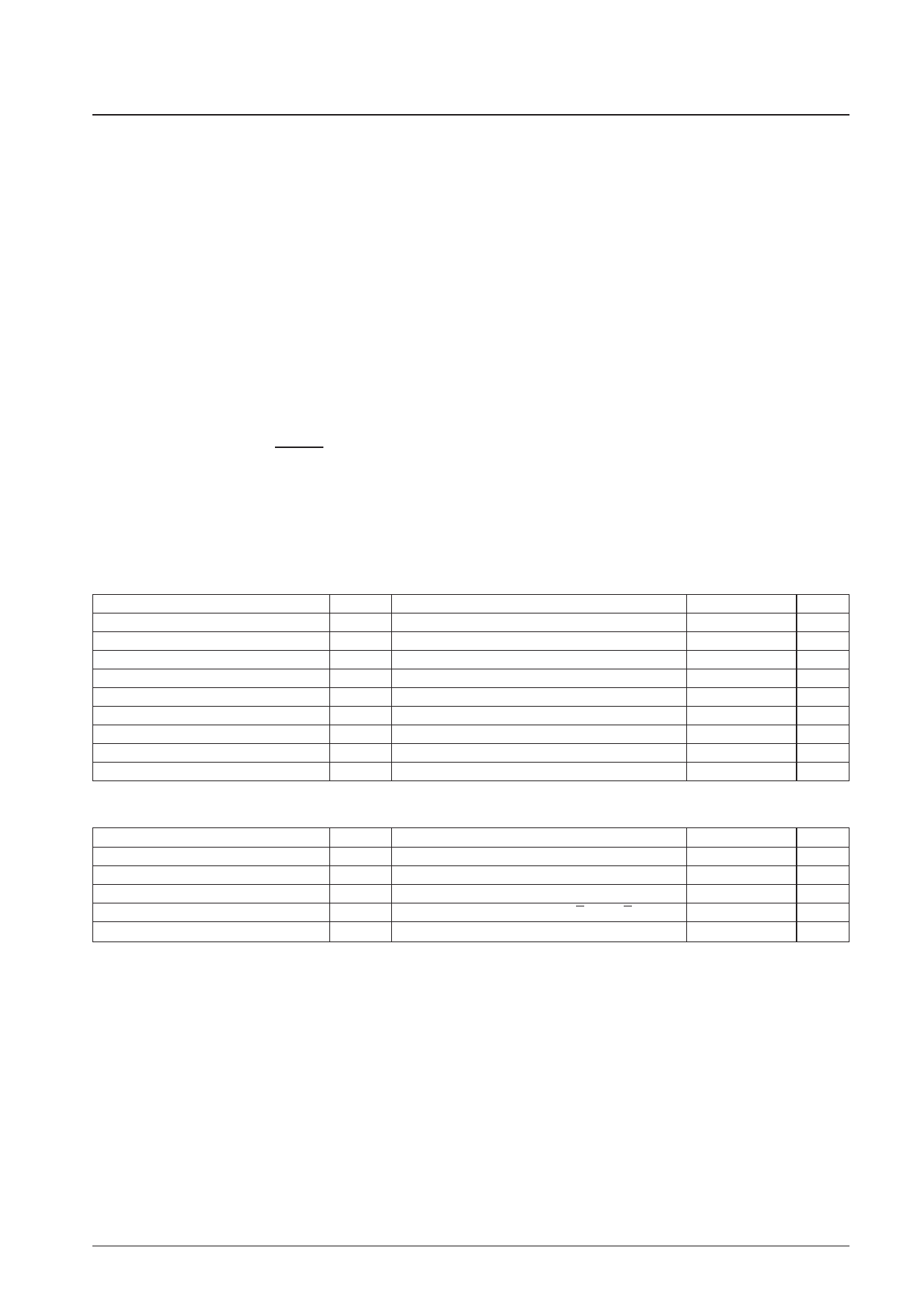
Absolute Maximum Ratings at Tc = 25°C
Parameter
Maximum supply voltage 1
Maximum supply voltage 2
Input voltage
Phase output current
Repeated avalanche resistance
Power dissipation
Operating IC substrate temperature
Junction temperature
Storage temperature
Symbol
VCC1 max
VCC2 max
VIN max
IOH max
Ear max
Pd max
Tc max
Tj max
Tstg
Conditions
No signal
No signal
Logic input pins
0.5 s, 1 pulse, when VCC1 applied
θc-a = 0
Allowable Operating Ranges at Ta = 25°C
Parameter
Supply voltage 1
Supply voltage 2
Input voltage
Phase drive voltage handling capacity
Phase current
Symbol
VCC1
VCC2
VIH
VDSS
IOH max
Conditions
When the input signal is present
When the input signal is present
Transistors 1, 2, 3, and 4 (outputs A, A, B, and B)
Duty 50%
Ratings
Unit
52
V
–0.3 to +7.0
V
–0.3 to +7.0
V
1.6
A
25
mJ
7
W
105
°C
150
°C
–40 to +125
°C
Ratings
Unit
10 to 45
V
5 ±5%
V
0 to VCC2
V
100 (min)
V
1.2 (max)
A
No. 7441-2/19
Share Link: