STK672-060 View Datasheet(PDF) - SANYO -> Panasonic
Part Name
Description
Manufacturer
STK672-060
SANYO -> Panasonic

STK672-060 Datasheet PDF : 19 Pages
| |||
IC Operation
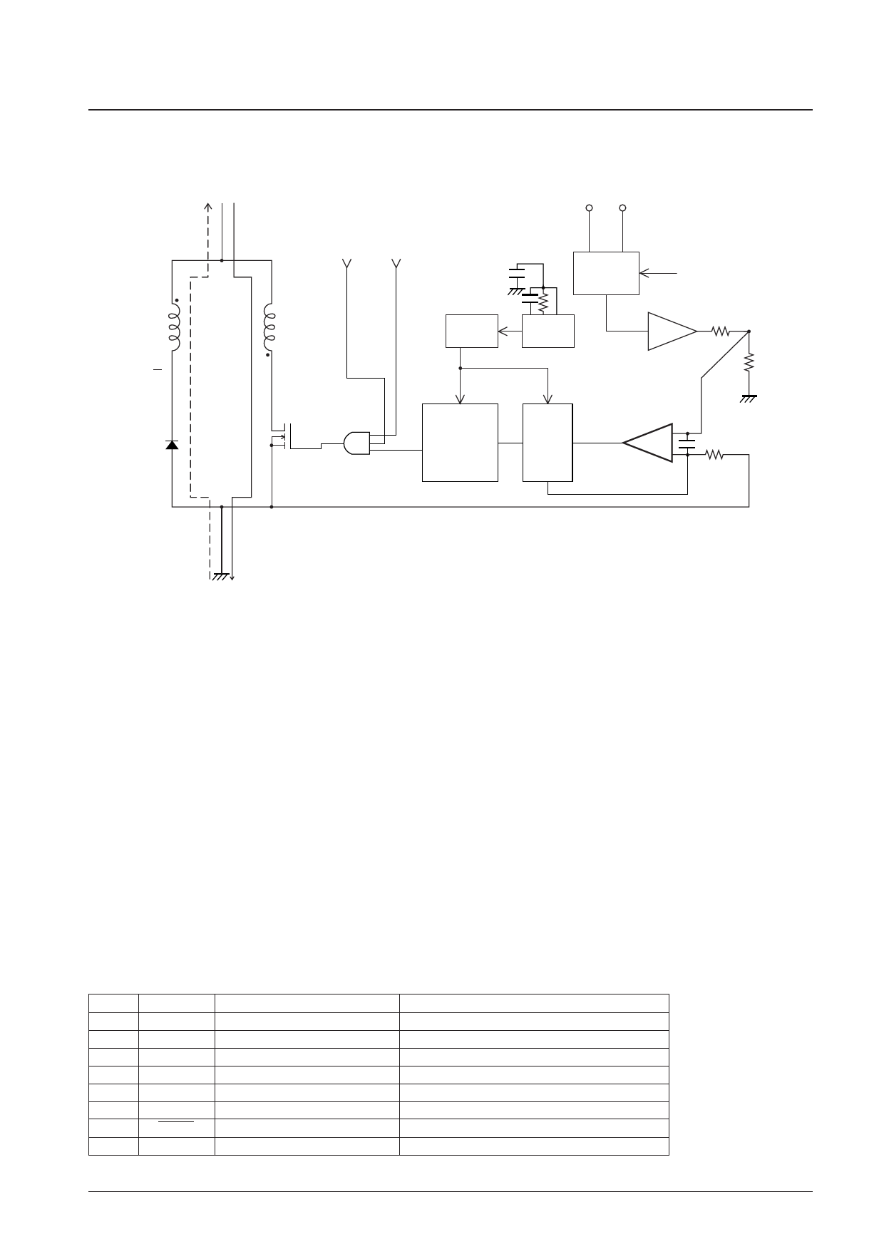
External Excitation Chopping Driver Block
VCC1
STK672-060
M4 M5
IOFF
L2
A
D1
ION
Enable øA (Control signal)
Current
divider
L1
A
MOSFET AND
Divider
45kHz
S
RC
oscillator
800kHz
Q Latch circuit
R Noise
filter
Vref
A=1
–
+
Rs
Driver Block Basic Circuit Structure
ITF02272
Since this hybrid IC adopts an external excitation method, no external oscillator circuit is required.
If a high level is input on the øA line in the driver block basic circuit in the figure and the MOSFET is turned on, the
comparator + input will go to the low level and the comparator output will go to the low level. Meanwhile, since the set
signal is input during the PMW period, the Q output will go to the high level and the initial state of the MOSFET will be
the on state.
The current ION that flows in the MOSFET will pass through L1 generating a potential difference across Rs. Then, when
the Rs potential becomes the same as the Vref potential, the comparator output will invert, the reset signal will be
generated, and the Q output will invert, into the low level. This turns the MOSFET off and the energy stored in L1 is
induced in L2, and IOFF is regenerated to the power supply. This state is maintained for the time that the set signal is
input to the latch circuit.
The Q output is turned on and off repeatedly by the set and reset signals in this manner, which implements constant
current control. The resistor and capacitor connected at the comparator input synchronize with the PWM period of the
spike absorption circuit.
Because of the fixed period due to the external excitation method adopted and synchronized PWM system, this circuit
can minimize hold noise generated when the motor position is locked.
Input Pin Description
Pin No.
14
15
17
18
9, 10, 11
12, 13
16
8
Pin
CLK
CWB
RETURN
ENABLE
M1, M2, M3
M4, M5
RESET
Vref
Function
Phase switching clock
Rotation direction setting (CW/CCW)
Forcible return to phase origin
Output cutoff
Excitation mode setting
Vector locus setting
System reset
Current value setting
Pin circuit type
CMOS Schmitt trigger circuit with built-in pull-up resistor
CMOS Schmitt trigger circuit with built-in pull-up resistor
CMOS Schmitt trigger circuit with built-in pull-up resistor
CMOS Schmitt trigger circuit with built-in pull-up resistor
CMOS Schmitt trigger circuit with built-in pull-up resistor
CMOS Schmitt trigger circuit with built-in pull-up resistor
CMOS Schmitt trigger circuit with built-in pull-up resistor
Operational amplifier input
No. 7441-8/19
Share Link: