ST7FLITEU05B3 View Datasheet(PDF) - STMicroelectronics
Part Name
Description
Manufacturer
ST7FLITEU05B3 Datasheet PDF : 115 Pages
| |||
ST7LITEU05 ST7LITEU09
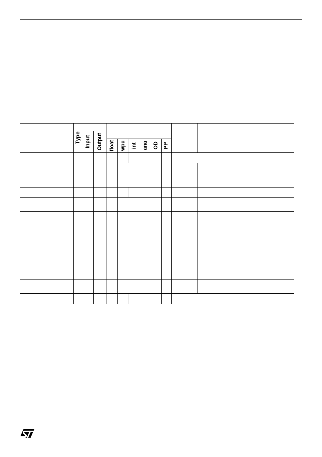
PIN DESCRIPTION (Cont’d)
Legend / Abbreviations for Table 2:
Type: I = input, O = output, S = supply
In/Output level: CT= CMOS 0.3VDD/0.7VDD with
input trigger
Output level: HS = High sink (on N-buffer only)
Port and control configuration:
– Input:float = floating, wpu = weak pull-up, int = in-
terrupt, ana = analog
– Output: OD = open drain, PP = push-pull
The RESET configuration of each pin is shown in
bold which is valid as long as the device is in reset
state.
Table 2. Device Pin Description
Pin
No.
Pin Name
Level
1 VDD 1)
2
PA5/AIN4/
CLKIN
S
I/O CT HS X
3 PA4/AIN3/MCO I/O CT HS X
4 PA3/RESET 2) O
5 PA2/AIN2/LTIC I/O CT HS X
6
PA1/AIN1/
ICCCLK
I/O CT HS X
7
PA0/AIN0/ATP-
WM/ICCDATA
I/O
CT
HS
X
8 VSS 1)
S
Port / Control
Main
Input
Output Function
(after
reset)
Alternate Function
Main power supply
ei4 X X X Port A5 Analog input 4 or External Clock Input
ei3
X
ei2
ei1
ei0
X X X Port A4 Analog input 3 or Main clock output
X X Port A3 RESET 2)
X
X
X Port A2
Analog input 2 or Lite Timer Input Cap-
ture
Analog input 1 or In Circuit Communica-
tion Clock
Caution: During normal operation this
pin must be pulled-up, internally or ex-
X X X Port A1 ternally (external pull-up of 10k manda-
tory in noisy environment). This is to
avoid entering ICC mode unexpectedly
during a reset. In the application, even if
the pin is configured as output, any re-
set will put it back in pull-up
X
X
X Port A0
Analog input 0 or Auto-Reload Timer
PWM or In Circuit Communication Data
Ground
Note:
1. It is mandatory to connect all available VDD and VDDA pins to the supply voltage and all VSS and VSSA
pins to ground.
2. After a reset, the multiplexed PA3/RESET pin will act as RESET. To configure this pin as output (Port
A3), write 55h to MUXCR0 and AAh to MUXCR1. For further details, please refer to section 7.4 on page
30.
7/115
1
Share Link: 