LT8330HS6 View Datasheet(PDF) - Linear Technology
Part Name
Description
Manufacturer
LT8330HS6 Datasheet PDF : 24 Pages
| |||
LT8330
Applications Information
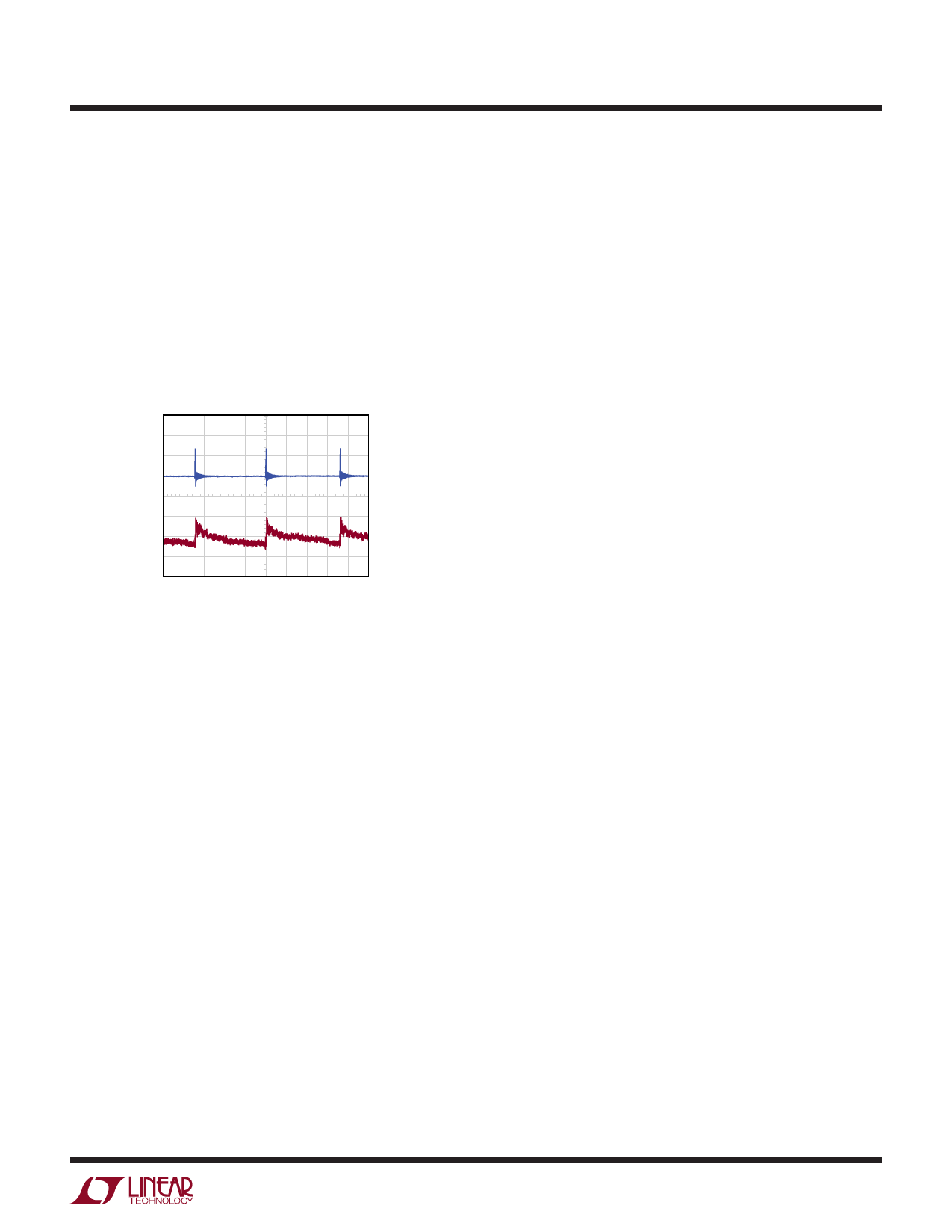
While in Burst Mode operation the current limit of the
switch is approximately 240mA resulting in the output
voltage ripple shown in Figure 2. Increasing the output
capacitance will decrease the output ripple proportionally.
As the output load ramps upward from zero the switch-
ing frequency will increase but only up to the fixed 2MHz
defined by the internal oscillator as shown in Figure 1. The
output load at which the LT8330 reaches the fixed 2MHz
frequency varies based on input voltage, output voltage,
and inductor choice.
INTVCC Regulator
A low dropout (LDO) linear regulator, supplied from VIN,
produces a 3V supply at the INTVCC pin. A minimum 1µF
low ESR ceramic capacitor must be used to bypass the
INTVCC pin to ground to supply the high transient currents
required by the internal power MOSFET gate driver.
No additional components or loading is allowed on this
pin. The INTVCC rising threshold (to allow soft start and
switching) is typically 2.6V. The INTVCC falling threshold
(to stop switching and reset soft start) is typically 2.5V.
Duty Cycle Consideration
IL
200mA/DIV
VOUT
5mV/DIV
The LT8330 minimum on-time, minimum off-time and
switching frequency (fOSC) define the allowable minimum
and maximum duty cycles of the converter (see Minimum
On-Time, Minimum Off-Time, and Switching Frequency
in the Electrical Characteristics table).
5µs/DIV
8330 F02
Figure 2. Burst Mode Operation
Programming Input Turn-On and Turn-Off
Thresholds with EN/UVLO Pin
The EN/UVLO pin voltage controls whether the LT8330 is
enabled or is in a shutdown state. A 1.6V reference and a
comparator A6 with built-in hysteresis (typical 80mV) allow
the user to accurately program the system input voltage
at which the IC turns on and off (see the Block Diagram).
The typical input falling and rising threshold voltages can
be calculated by the following equations:
VIN(FALLING,UVLO(–)) = 1.60 • (R3+R4)/R4
VIN(RISING, UVLO(+)) = 1.68 • (R3+R4)/R4
VIN current is reduced below 1µA when the EN/UVLO pin
voltage is less than 0.2V. The EN/UVLO pin can be con-
nected directly to the input supply VIN for always-enabled
operation. A logic input can also control the EN/UVLO pin.
When operating in Burst Mode operation for light load
currents, the current through the R3 and R4 network can
easily be greater than the supply current consumed by the
LT8330. Therefore, R3 and R4 should be large enough to
minimize their effect on efficiency at light loads.
Minimum Allowable Duty Cycle =
Minimum On-Time(MAX) • fOSC(MAX)
Maximum Allowable Duty Cycle =
1 – Minimum Off-Time(MAX) • fOSC(MAX)
The required switch duty cycle range for a Boost converter
operating in continuous conduction mode (CCM) can be
calculated as:
DMIN = 1– VIN(MAX)/(VOUT + VD)
DMAX = 1– VIN(MIN)/(VOUT + VD)
where VD is the diode forward voltage drop. If the above
duty cycle calculations for a given application violate the
minimum and/or maximum allowed duty cycles for the
LT8330, operation in discontinuous conduction mode
(DCM) might provide a solution. For the same VIN and
VOUT levels, operation in DCM does not demand as low a
duty cycle as in CCM. DCM also allows higher duty cycle
operation than CCM. The additional advantage of DCM is
the removal of the limitations to inductor value and duty
cycle required to avoid sub-harmonic oscillations and the
right half plane zero (RHPZ). While DCM provides these
benefits, the trade-off is higher inductor peak current, lower
available output power and reduced efficiency.
8330fa
For more information www.linear.com/LT8330
9
Share Link: 