AD722 View Datasheet(PDF) - Analog Devices
Part Name
Description
Manufacturer
AD722 Datasheet PDF : 12 Pages
| |||
AD722
+5V (VAA)
+5V (VCC)
MPEG
DECODER
+5V (VAA)
0.1µF
24
DATA IN
VAA
COMP
VREF
FSADJ
+5V (VAA) ADV7120
10kΩ
SYNC
IOR
0.01µF
0.1µF
+5V
0.1µF
0.1µF
RSET
550Ω
AD589
(1.2V REF)
0.01µF
+5V
10kΩ
4
APOS
5 ENCD
14
DPOS
L1 (FERRITE BEAD)
10µF
33µF
GND
+5V
AD722
10kΩ
12 SELECT
+ 75Ω
COMP 10
6 RIN
220µF
COMPOSITE
VIDEO
CLOCK
IOG
BLANK
GND IOB
75Ω 75Ω 75Ω
75Ω 75Ω 75Ω
HSYNC
VSYNC
* PARALLEL–RESONANT
CRYSTAL; 3.579545MHz (NTSC)
OR 4.433620MHz (PAL)
CAPACITOR VALUE DEPENDS ON
CRYSTAL CHOSEN
+5V
0.1µF
**FSC OR 4FSC CLOCK; 3.579545MHz,
14.31818MHz (NTSC) OR 4.433620MHZ,
17.734480MHz(PAL)
OSC **
*
CRYSTAL
HSYNC
VSYNC
10–30pF
7 GIN
8 BIN
+ 75Ω
LUMA 11
220µF
16 HSYNC
+ 75Ω
CRMA 9
220µF
15 VSYNC
+5V
3 FIN
DGND
13
STND 1
AGND
2
10kΩ
S-VIDEO
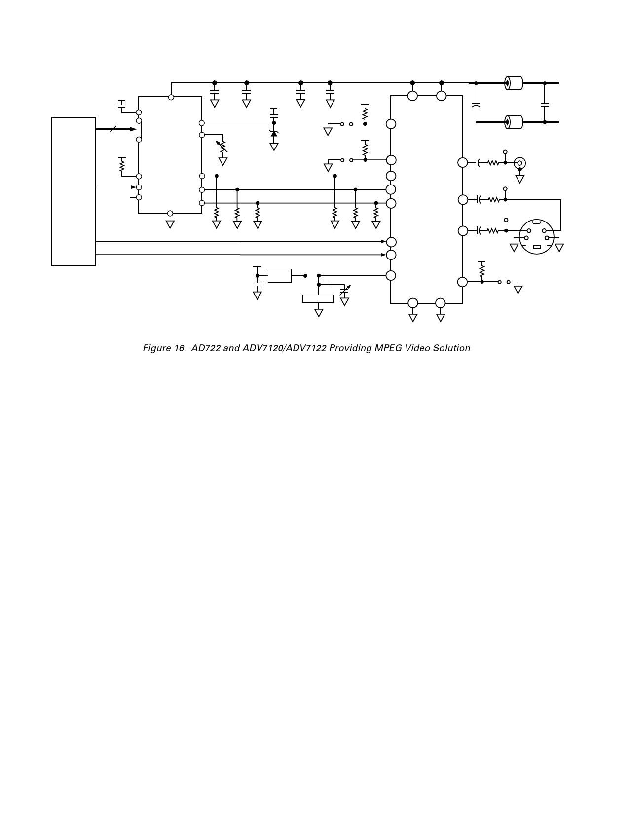
Figure 16. AD722 and ADV7120/ADV7122 Providing MPEG Video Solution
Figure 15 shows a circuit for connection to the VGA port of a
PC. The RGB outputs connect directly to the respective inputs
of the AD722. These signals should each be terminated to
ground with 75 Ω.
The standard 15-pin VGA connector has HSYNC on Pin 13
and VSYNC on Pin 14. These signals also connect directly to
the same name signals on the AD722. The FIN signal can be
provided by any of the means described elsewhere in the data
sheet. For a synchronous NTSC system, the internal 4FSC
(14.31818 MHz) clock that drives the VGA controller can be
used for FIN on the AD722. This signal is not directly accessible
from outside the computer, but it does appear on the VGA card.
If a separate RGB monitor is also to be used, it is not possible to
simply connect it to the R, G, and B signals. The monitor pro-
vides a termination that would double terminate these signals.
The R, G, and B signals should be buffered by three amplifiers
with high input impedances. These should be configured for a
gain of two, which is normalized by the divide by two termina-
tion scheme used for the RGB monitor.
The AD813 is a triple video amplifier that can provide the nec-
essary buffering in a single package. It also provides a disable
pin for each amplifier which can be used to disable the drive to
the RGB monitor when interlaced video is used (SELECT = LO).
When the RGB signals are noninterlaced, setting SELECT HI will
enable the AD813 to drive the RGB monitor and disable the en-
coding function of the AD722 via Pin 5. HSYNC and VSYNC
are logic level signals that can drive both the AD722 and RGB
monitor in parallel.
AD722 Used with an MPEG Decoder
MPEG decoding of compressed video signals is becoming a
more prevalent feature in many PC systems. To display images
on the computer monitor, video in RGB format is required.
However, to display the images on a TV monitor or to record
the images on a VCR, video in composite format is required.
Figure 16 shows a schematic for taking the 24-bit wide RGB
video from an MPEG decoder and creating both analog RGB
video and composite video.
The 24-bit wide RGB video is converted to analog RGB by the
ADV7120 (Triple 8-bit video DAC–available in 48-pin TQFP).
The analog current outputs from the DAC are terminated to
ground at both ends with 75 Ω as called for in the data sheet.
These signals directly feed the analog inputs of the AD722. The
HSYNC and VSYNC signals from the MPEG Controller are di-
rectly applied to the AD722.
If the set of termination resistors closest to the AD722 are re-
moved, an RGB monitor can be connected to these signals and
it will provide the required second termination. This scenario is
acceptable as long as the RGB monitor is always present and
connected. If it is to be removed on occasion, another termina-
tion scheme is required.
The AD813 triple video op amp can provide buffering for such
applications. Each channel is set for a gain of two while the out-
puts are back terminated with a series 75 Ω resistor. This pro-
vides the proper signal levels at the monitor which terminates
the lines with 75 Ω.
AD722 APPLICATION DISCUSSION
Chrominance and Luminance Alignment
Inside the AD722 the chrominance and luminance signals are pro-
cessed by separate paths. They both are either output separately
(Y/C), or they are added together by the composite video ampli-
fier. Although both channels are filtered, the chrominance signal
experiences a greater filtering delay due to the higher order of
the chrominance path filters. To compensate, a sampled delay
line is used in the luminance path.
For baseband video it is desirable for the chrominance and lu-
minance to be accurately aligned with zero offset. However, the
situation for modulated RF video is a bit more complicated due
to the effects of the IF circuitry used in TV sets.
–10–
REV. 0
Share Link: 