AD722 View Datasheet(PDF) - Analog Devices
Part Name
Description
Manufacturer
AD722 Datasheet PDF : 12 Pages
| |||
AD722
H TIMING MEASUREMENT RS–170A (NTSC)
FIELD = 1 LINE = 22
5.49µs
4.59µs
9.72µs
9.0 CYCLES
H TIMING (PAL)
LINE = 25
4.60µs
5.59µs
2.28µs
100ns
124ns
AVERAGE 256 ≥ 256
39.7 IRE
33.8 IRE
94ns
102ns
AVERAGE 256 ≥ 256
293.5mV
249.0mV
Figure 12. Horizontal Timing, NTSC
Figure 13. Horizontal Timing, PAL
SUB-
CARRIER
FSC
4FSC
NTSC/PAL
HSYNC
VSYNC
XOSC
PHASE
DETECTOR
CHARGE
PUMP
FILTER
LOOP
4FSC
VCO
4FSC
XNOR
SYNC
SEPARATOR
FSC
BURST
CSYNC
NTSC/PAL
4FSC
CSYNC
QUADRATURE
+4
DECODER
FSC 90°
FSC 0°
±180°
SC 90°/270°
(PAL ONLY)
BURST
POWER AND GROUNDS
+5V
LOGIC
+5V
ANALOG
AGND
ANALOG
DGND
LOGIC
NTSC/PAL
CLOCK
AT 4FSC
NOTE:
THE LUMINANCE, COMPOSITE, AND
CHROMINANCE OUTPUTS ARE AT
TWICE NORMAL LEVELS FOR DRIVING
75Ω REVERSE-TERMINATED LINES.
RED
DC
CLAMP
GREEN
DC
CLAMP
BLUE
DC
CLAMP
Y 3-POLE
LP PRE-
FILTER
RGB-TO-YUV U
ENCODING
4-POLE
MATRIX
LPF
U
CLAMP
V
4-POLE
LPF
V
CLAMP
CSYNC
INSERTION
SAMPLED-
DATA
DELAY
LINE
5 MHz
2-POLE
LP POST-
FILTER
NTSC/PAL
BALANCED
MODULATORS
3-POLE LPF
3.6MHz (NTSC)
4.4MHz (PAL)
LUMINANCE
X2
OUTPUT
X2
COMPOSITE
OUTPUT
CHROMINANCE
X2
OUTPUT
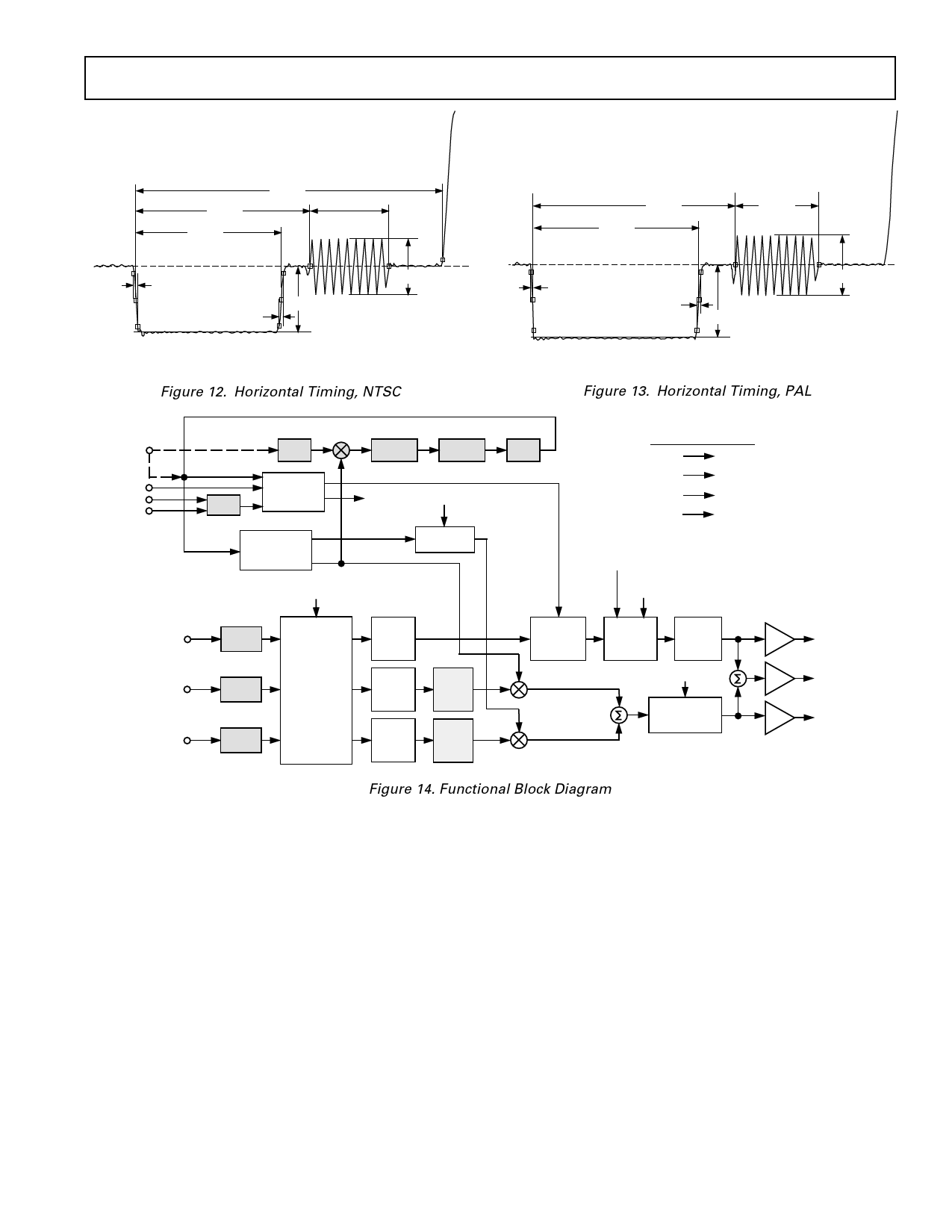
Figure 14. Functional Block Diagram
THEORY OF OPERATION
The AD722 was designed to have three allowable modes of ap-
plying a clock via the FIN pin. These are FSC (frequency of
subcarrier, 3.579545 MHz for NTSC or 4.433618 MHz for
PAL) mode with CMOS clock applied, FSC mode using on-
chip crystal oscillator, and 4FSC mode with CMOS clock ap-
plied. To use FSC mode SELECT is pulled low and then either
a CMOS FSC clock is applied to FIN, or a parallel-resonant
crystal and appropriate tuning capacitor is placed between FIN
pin and GND to utilize the on-chip oscillator. The on-chip
Phase Locked Loop (PLL) is used in these modes to generate an
internal 4FSC which is divided to perform the digital clocking
as well as to create the quadrature subcarrier signals for the
chrominance modulation. In 4FSC mode the PLL is bypassed.
Referring to the AD722 block diagram (Figure 14), the RGB in-
puts (each 714 mV p-p max for NTSC or 700 mV p-p max for
PAL) are ac-coupled and then pass through dc clamps. These
clamps allow the user to have a black level which is not at 0 V.
The clamps will clamp to a black input signal level between 0 V
and 3 V. The clamping occurs just after the falling edge of
HSYNC.
The RGB inputs then pass into an analog encoding matrix
which creates the luminance (“Y”) signal and the chrominance
color difference (“U” and “V”) signals. The RGB to YUV en-
coding is performed using the following standard transformation:
Y = 0.299 × R + 0.587 × G + 0.114 × B
U = 0.493 × (B–Y)
V = 0.877 × (R–Y)
After the encoding matrix, the AD722 has two parallel analog
paths. The Y (luminance) signal is first passed through a 3-pole
4.85 MHz/6 MHz (NTSC/PAL) Bessel low-pass filter to pre-
vent aliasing in the sampled-data delay line. This first low-pass
filter is also where the unclocked analog sync signal is injected
into the Y signal (more on the creation of this sync signal to fol-
low). The Y signal then passes through the sampled-data delay
line, which is clocked at 4FSC. The delay line was designed to
give an overall chrominance to luminance delay of –170 ns. Fol-
lowing the sampled-data delay line is a 5.25 MHz/6.5 MHz
(NTSC/PAL) 2-pole low-pass Bessel filter to smooth the recon-
structed luminance signal.
REV. 0
–7–
Share Link: 