PEEL18CV8 View Datasheet(PDF) - International Cmos Technology
Part Name
Description
Manufacturer
PEEL18CV8 Datasheet PDF : 10 Pages
| |||
® International
CMOS
Technology
PEELTM 18CV8
A.C. Electrical Characteristics
Over the operating range 8
Symbol
Parameter
tPD
tOE
tOD
tCO1
tCO2
tCF
tSC
tHC
tCL, tCH
tCP
fMAX1
fMAX2
fMAX3
tAW
tAP
tAR
tRESET
Input5 to non-registered output
Input5 to output enable6
Input5 to output disable6
Clock to Output
Clock to comb. output delay
via internal registered feedback
Clock to Feedback
Input5 or feedback setup to clock
Input5 hold after clock
Clock low time, clock high time8
Min clock period Ext (tSC + tCO1)
Internal feedback (1/tSC+tCF)11
External Feedback (1/tCP)11
No Feedback (1/tCL+tCH)11
Asynchronous Reset Pulse Width
Input5 to Asynchronous Reset
Asynchronous Reset recovery time
Power-on reset time for registers
in clear state
-5
-7
-10/I-10 -15/I-15 -25/I-25
Units
Min Max Min Max Min Max Min Max Min Max
5
7.5
10
15
25
ns
5
7.5
10
15
25
ns
5
7.5
10
15
25
ns
4
7
7
12
15
ns
7.5
10
12
25
35
ns
2.5
3.5
4
8
15
ns
3.5
5
5
12
20
ns
0
0
0
0
0
ns
3
3.5
5
10
15
ns
7
12
12
24
35
166.7
117.6
111
50
28.5
ns
MHz
133
83.3
83.3
41.6
28.5
MHz
166.7
142.8
100
50
33.3
MHz
5
7.5
10
15
25
ns
5
7.5
10
15
25
ns
5
7.5
10
15
25
ns
5
5
5
5
5
µs
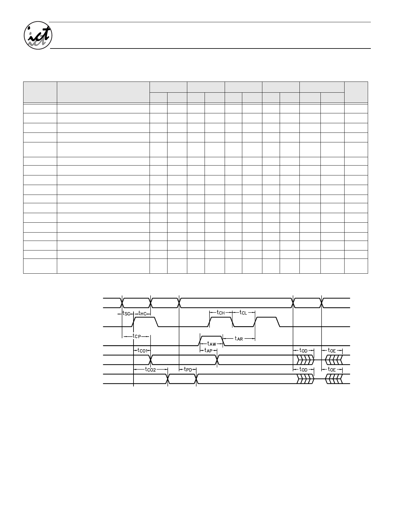
Switching Waveforms
Inputs, I/O,
Registered Feedback,
Synchronous Preset
Clock
Asynchronous
Reset
Registered
Outputs
Combinatorial
Outputs
Notes:
1. Minimum DC input is -0.5V, however, inputs may undershoot to -2.0V
for periods less than 20 ns.
2. VI and VO are not specified for program/verify operation.
3. Test Points for Clock and VCC in tR and tF are referenced at the 10%
and 90% levels.
4. I/O pins are 0V and VCC.
5. “Input” refers to an input pin signal.
6. tOE is measured from input transition to VREF±0.1V, TOD is measured
from input transition to VOH-0.1V or VOL+0.1V; VREF=VL.
7. Capacitances are tested on a sample basis.
8. Test conditions assume: signal transition times of 3ns or less from the
10% and 90% points, timing reference levels of 1.5V (Unless otherwise
specified).
9. Test one output at a time for a duration of less than 1 second.
10. ICC for a typical application: This parameter is tested with the device
programmed as an 8-bit Counter.
11. Parameters are not 100% tested. Specifications are based on initial
characterization and are tested after any design process modification that
might affect operational frequency.
12. Available only for 18CV8 -15/I-15/-25/I-25 grades
13. 24mA available for 18CV8-5/-7. All other speeds are 16mA.
7
04-02-004H
Share Link: 