SST25VF032B View Datasheet(PDF) - Silicon Storage Technology
Part Name
Description
Manufacturer
SST25VF032B Datasheet PDF : 28 Pages
| |||
32 Mbit SPI Serial Flash
SST25VF032B
Data Sheet
INSTRUCTIONS
Instructions are used to read, write (Erase and Program),
and configure the SST25VF032B. The instruction bus
cycles are 8 bits each for commands (Op Code), data, and
addresses. The Write-Enable (WREN) instruction must be
executed prior any Byte-Program, Auto Address Increment
(AAI) programming, Sector-Erase, Block-Erase, Write-Sta-
tus-Register, or Chip-Erase instructions. The complete list
of instructions is provided in Table 5.
All instructions are synchronized off a high to low transition
of CE#. Inputs will be accepted on the rising edge of SCK
starting with the most significant bit. CE# must be driven
low before an instruction is entered and must be driven
high after the last bit of the instruction has been shifted in
(except for Read, Read-ID, and Read-Status-Register
instructions). Any low to high transition on CE#, before
receiving the last bit of an instruction bus cycle, will termi-
nate the instruction in progress and return the device to
standby mode. Instruction commands (Op Code),
addresses, and data are all input from the most significant
bit (MSB) first.
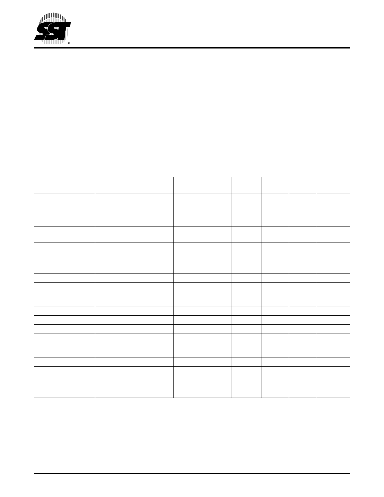
TABLE 5: Device Operation Instructions
Instruction
Description
Op Code Cycle1
Address Dummy Data Maximum
Cycle(s)2 Cycle(s) Cycle(s) Frequency
Read
Read Memory
0000 0011b (03H)
3
0
1 to ∞ 25 MHz
High-Speed Read
Read Memory at higher speed 0000 1011b (0BH)
3
1
1 to ∞ 80 MHz
4 KByte Sector-Erase3 Erase 4 KByte of
memory array
0010 0000b (20H)
3
0
0
80 MHz
32 KByte Block-Erase4 Erase 32KByte block
of memory array
0101 0010b (52H)
3
0
0
80 MHz
64 KByte Block-Erase5 Erase 64 KByte block
of memory array
1101 1000b (D8H)
3
0
0
80 MHz
Chip-Erase
Erase Full Memory Array
0110 0000b (60H) or
0
1100 0111b (C7H)
0
0
80 MHz
Byte-Program
To Program One Data Byte 0000 0010b (02H)
3
0
1
80 MHz
AAI-Word-Program6 Auto Address Increment
1010 1101b (ADH)
3
Programming
0
2 to ∞ 80 MHz
RDSR7
Read-Status-Register
0000 0101b (05H)
0
0
1 to ∞ 80 MHz
EWSR
Enable-Write-Status-Register 0101 0000b (50H)
0
0
0
80 MHz
WRSR
Write-Status-Register
0000 0001b (01H)
0
0
1
80 MHz
WREN
Write-Enable
0000 0110b (06H)
0
0
0
80 MHz
WRDI
Write-Disable
0000 0100b (04H)
0
0
0
80 MHz
RDID8
Read-ID
1001 0000b (90H) or
3
1010 1011b (ABH)
0
1 to ∞ 80 MHz
JEDEC-ID
JEDEC ID read
1001 1111b (9FH)
0
0
3 to ∞ 80 MHz
EBSY
Enable SO as an output RY/BY# 0111 0000b (70H)
0
status during AAI programming
0
0
80 MHz
DBSY
Disable SO as an output RY/BY# 1000 0000b (80H)
0
status during AAI programming
0
0
80 MHz
T5.0 1327
1. One bus cycle is eight clock periods.
2. Address bits above the most significant bit can be either VIL or VIH.
3. 4KByte Sector Erase addresses: use AMS-A12, remaining addresses are don’t care but must be set either at VIL or VIH.
4. 32KByte Block Erase addresses: use AMS-A15, remaining addresses are don’t care but must be set either at VIL or VIH.
5. 64KByte Block Erase addresses: use AMS-A16, remaining addresses are don’t care but must be set either at VIL or VIH.
6. To continue programming to the next sequential address location, enter the 8-bit command, ADH, followed by 2 bytes of data to be
programmed. Data Byte 0 will be programmed into the initial address [A23-A1] with A0=0, Data Byte 1 will be programmed into the
initial address [A23-A1] with A0 = 1.
7. The Read-Status-Register is continuous with ongoing clock cycles until terminated by a low to high transition on CE#.
8. Manufacturer’s ID is read with A0 = 0, and Device ID is read with A0 = 1. All other address bits are 00H. The Manufacturer’s ID and
device ID output stream is continuous until terminated by a low-to-high transition on CE#.
©2009 Silicon Storage Technology, Inc.
8
S71327-03-000
05/09
Share Link: 