M38047F5KP View Datasheet(PDF) - Renesas Electronics
Part Name
Description
Manufacturer
M38047F5KP Datasheet PDF : 116 Pages
| |||
3804 Group (Spec. H)
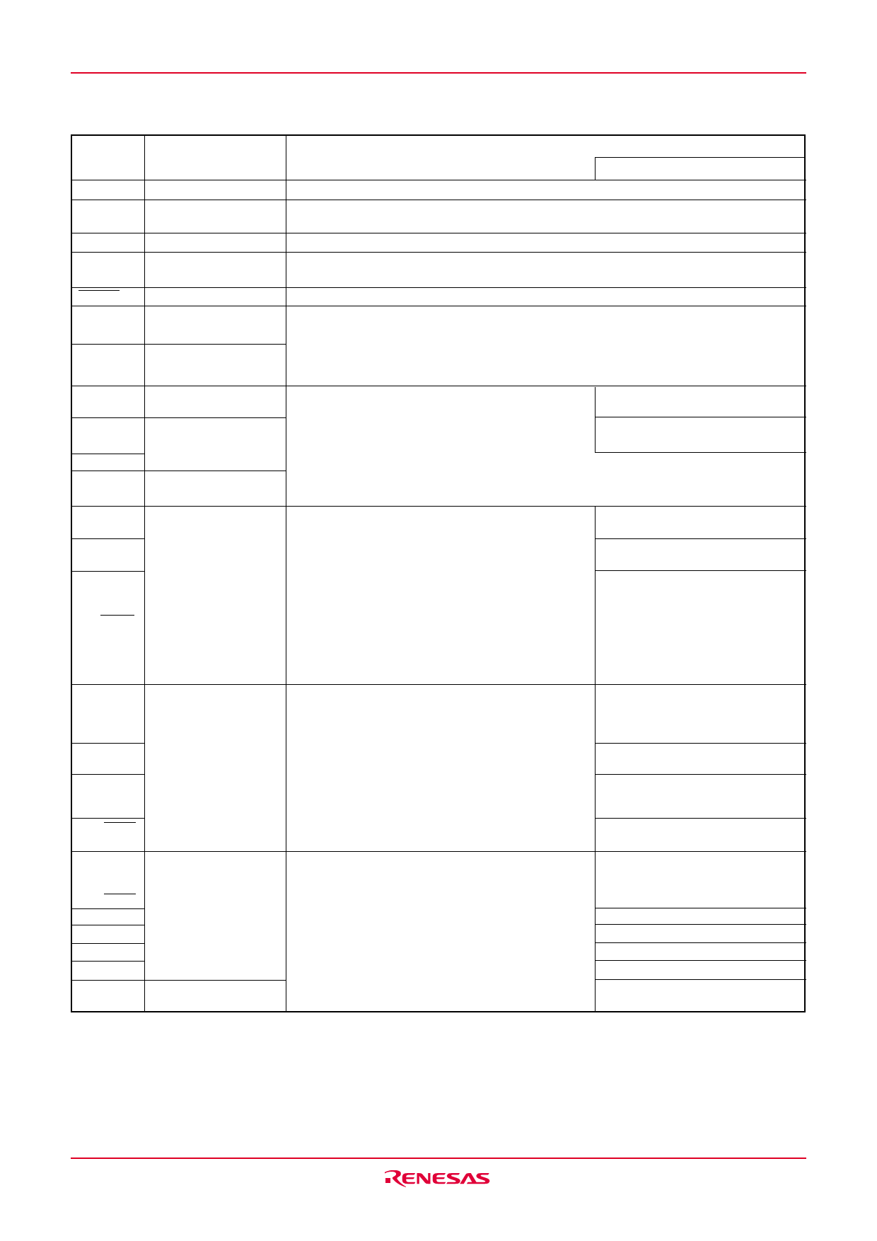
PIN DESCRIPTION
Table 2 Pin description
Pin
VCC, VSS
CNVSS
Name
Power source
CNVSS input
VREF
AVSS
Reference voltage
Analog power source
RESET
XIN
Reset input
Clock input
XOUT
Clock output
P00/AN8–
P07/AN15
P10/INT41
P11/INT01
P12–P17
P20–P27
I/O port P0
I/O port P1
I/O port P2
P30/DA1
P31/DA2
P32/SDA
P33/SCL
P34/RxD3
P35/TxD3
P36/SCLK3
P37/SRDY3
I/O port P3
P40/INT40/
XCOUT
P41/INT00/
XCIN
P42/INT1
P43/INT2
P44/RxD1
P45/TxD1
P46/SCLK1
P47/SRDY1
/CNTR2
P50/SIN2
P51/SOUT2
P52/SCLK2
P53/SRDY2
P54/CNTR0
P55/CNTR1
P56/PWM
P57/INT3
P60/AN0–
P67/AN7
I/O port P4
I/O port P5
I/O port P6
Functions
Function except a port function
•Apply voltage of 2.7 V–5.5 V to Vcc, and 0 V to Vss.
•This pin controls the operation mode of the chip.
•Normally connected to VSS.
•Reference voltage input pin for A/D and D/A converters.
•Analog power source input pin for A/D and D/A converters.
•Connect to VSS.
•Reset input pin for active “L”.
•Input and output pins for the clock generating circuit.
•Connect a ceramic resonator or quartz-crystal oscillator between the XIN and XOUT pins to set
the oscillation frequency.
•When an external clock is used, connect the clock source to the XIN pin and leave the XOUT
pin open.
•8-bit CMOS I/O port.
•A/D converter input pin
•I/O direction register allows each pin to be individually
programmed as either input or output.
•Interrupt input pin
•CMOS compatible input level.
•CMOS 3-state output structure.
•Pull-up control is enabled in a bit unit.
•P20–P27 are enabled to output large current for LED drive.
•8-bit CMOS I/O port.
•D/A converter input pin
•I/O direction register allows each pin to be individually
programmed as either input or output.
•I2C-BUS interface function pins
•CMOS compatible input level.
•P32 to P33 can be switched between CMOS compat- •Serial I/O3 function pin
ible input level or SMBUS input level in the I2C-BUS
interface function.
•P30, P31, P34–P37 are CMOS 3-state output structure.
•P32, P33 are N-channel open-drain output structure.
•Pull-up control of P30, P31, P34–P37 is enabled in a bit
unit.
•8-bit CMOS I/O port.
•Interrupt input pin
•I/O direction register allows each pin to be individually •Sub-clock generating I/O pin
programmed as either input or output.
(resonator connected)
•CMOS compatible input level.
•Interrupt input pin
•CMOS 3-state output structure.
•Pull-up control is enabled in a bit unit.
•Serial I/O1 function pin
•Serial I/O1, timer Z function pin
•8-bit CMOS I/O port.
•I/O direction register allows each pin to be individually
programmed as either input or output.
•CMOS compatible input level.
•CMOS 3-state output structure.
•Pull-up control is enabled in a bit unit.
•Serial I/O2 function pin
•Timer X function pin
•Timer Y function pin
•PWM output pin
•Interrupt input pin
•A/D converter input pin
Rev.1.01 Jan 25, 2005 page 4 of 114
REJ03B0131-0101Z
Share Link: 