LB1821 View Datasheet(PDF) - SANYO -> Panasonic
Part Name
Description
Manufacturer
LB1821 Datasheet PDF : 16 Pages
| |||
LB1821M
Output system ground ... Ground for Rf and the output diodes
Signal system ground ... Ground for the IC and the IC external components
15. VREG Pin
If a motor drive system is formed from a single power supply, the VREG pin (pin 33) can be used to create the power-
supply voltage (about 6.3 V) for this IC. The VREG pin is a shunt regulator and generates a voltage of about 7 volts by
passing a current through an external resistor. A stable voltage can be generated by setting the current to value in the
range 1 to 7 mA. The external transistors must have current capacities of at least 80 mA (to cover the ICC + Hall bias
current + output current <source> requirements) and they must have voltage handling capacities in excess of the
motor power-supply voltage. Since the heat generated by these transistor may be a problem, heat sinks may be
required depending on the packages used. If the IC power-supply voltage (4.4 to 7.0 V) is provided from an external
circuit, apply that voltage directly to the VCC pin(pin 32). In that case, the VREG pin must either be left open or
connected to ground.
16. FG Amplifier
Normally, the FG amplifier is used to construct a filter amplifier such as that shown in the application circuit to reject
noise. Since a Schmitt comparator is connected after the FG amplifier, applications must set the amplification so that
the amplifier output amplitude is at least 250 mV p-p. (However, a setting that results in an amplitude of 1 to 3 V p-p
during steady-state rotation is desirable.) The capacitor connected between the FGIN+ pin (pin 15) and ground is
required for bias voltage stabilization and to generate the initial reset pulse for the internal logic. The reset pulse is
generated in the time it takes for the FGIN+ pin to go from 0 to about 1.3 V.
17. Integrating Amplifier
The integrating amplifier integrates the speed error pulses and the phase error pulses and converts them to a speed
command voltage. At the same time it also sets the control loop gain and frequency characteristics using external
components. The integrating amplifier output (pin 1) is normally connected to the TOC pin (pin 44) by an external
line. Separating the integrating amplifier output and the PWM control circuit allows applications to switch the
integrating amplifier constants using an external operational amplifier, analog switch, or other circuit. This is useful
in applications that require integration constant switching due to a wide range of variability in the motor speeds that
must be provided.
18. VCO Filter Amplifier
The VCO filter amplifier converts the VCO system PLL output to the VCO voltage. The amplifier input resistor
(about 10 kΩ) is built in. Therefore, the gain and the frequency characteristics are set by the feedback resistor and the
feedback capacitor. Since the range of frequency variation supported becomes narrower as the gain is reduced, it is
desirable to set the gain of this amplifier to be 1 or higher.
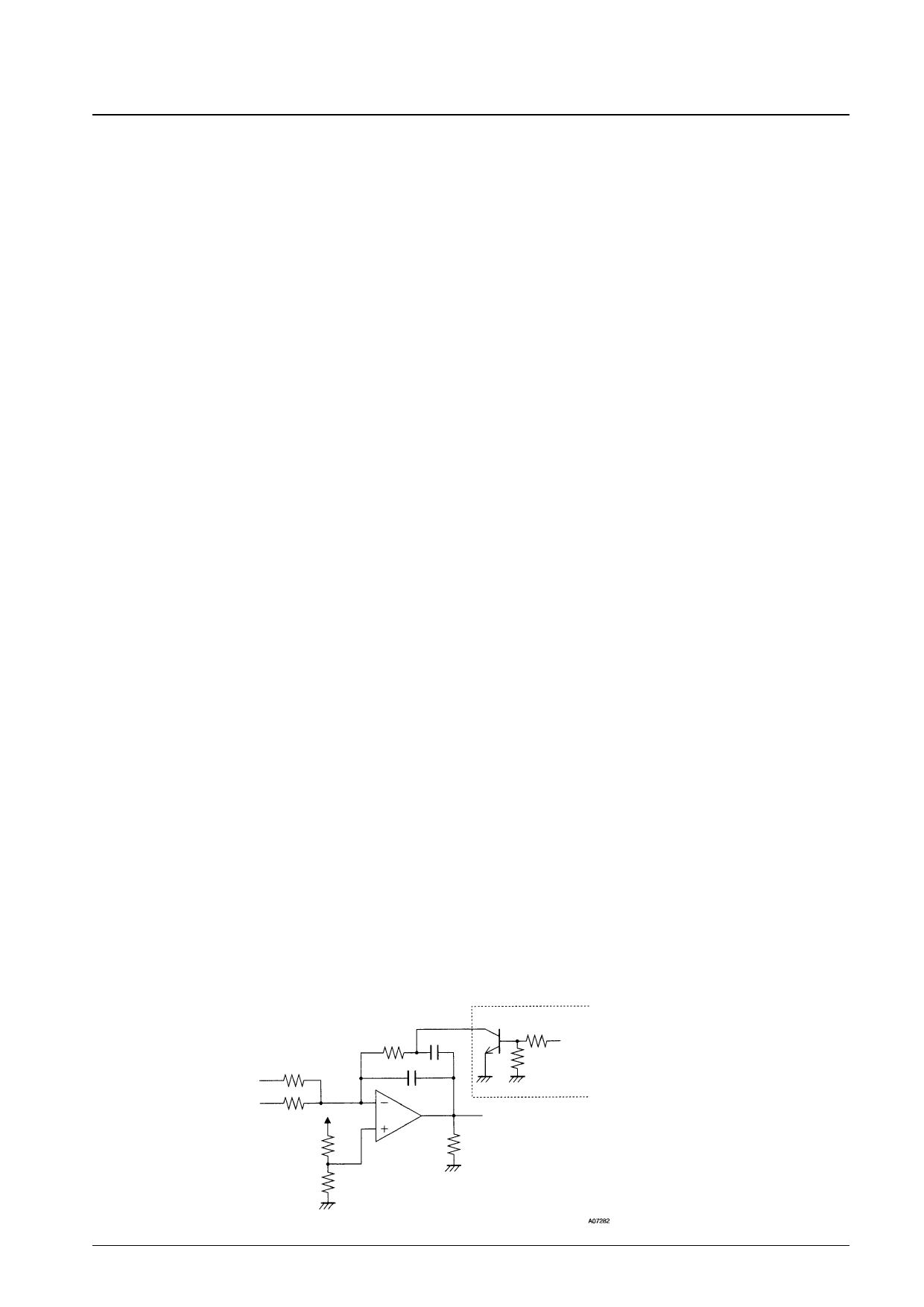
19. Startup Techniques
If the motor is started and stopped repeatedly over a short period, the charge accumulated on the integrating
amplifier’s external capacitor may become a problem. (This can result in abnormal speed overshooting at startup and
other problems.) The circuit shown below can be effective at resolving this problem.
Added circuit
S/S signal
No. 5686-10/16
Share Link: 