APA300-CQ View Datasheet(PDF) - Unspecified
Part Name
Description
Manufacturer
APA300-CQ Datasheet PDF : 174 Pages
| |||
ProASICPLUS Flash Family FPGAs
ProASICPLUS Architecture
The proprietary ProASICPLUS architecture provides
granularity comparable to gate arrays.
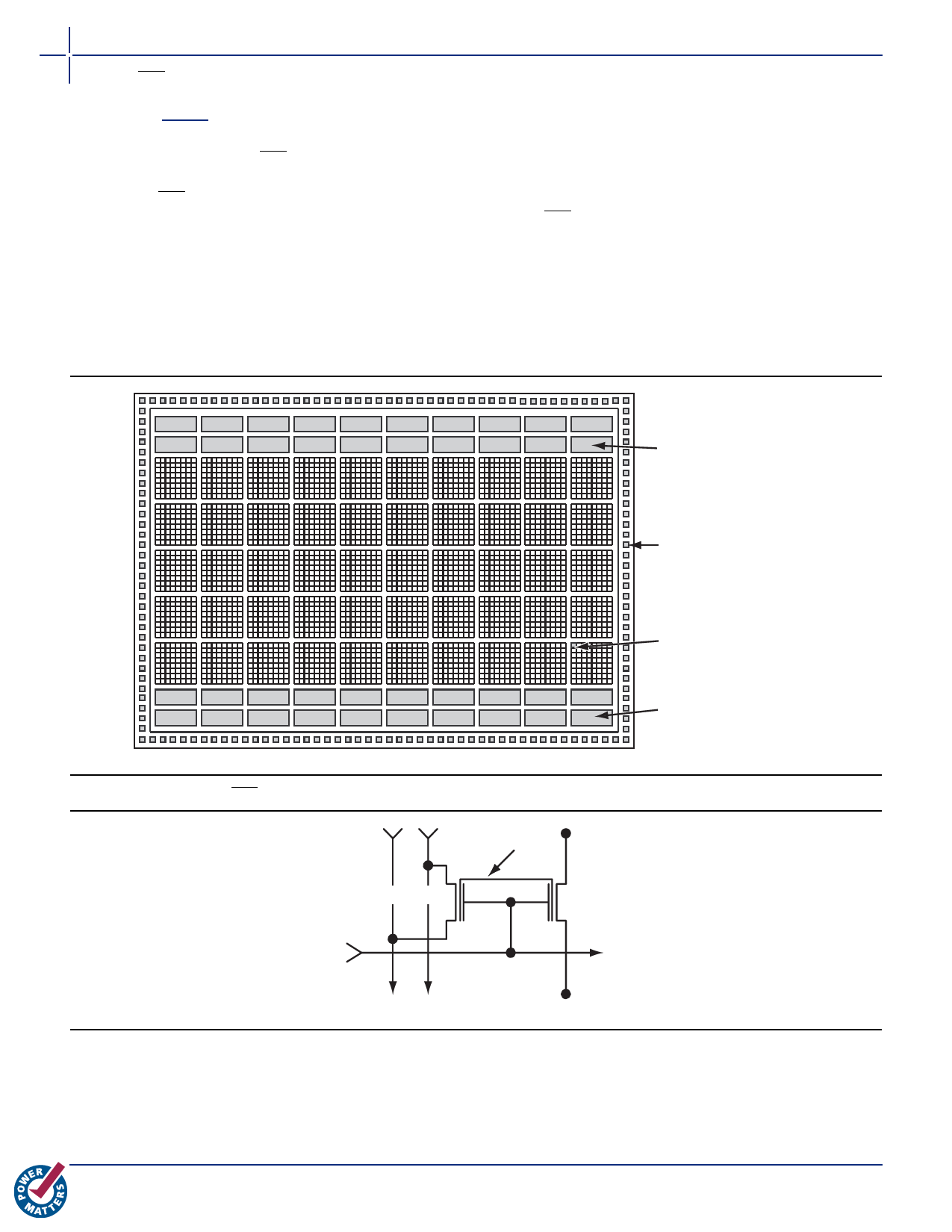
The ProASICPLUS device core consists of a Sea-of-Tiles
(Figure 1-1). Each tile can be configured as a three-input
logic function (e.g., NAND gate, D-Flip-Flop, etc.) by
programming the appropriate Flash switch
interconnections (Figure 1-2 and Figure 1-3 on page 1-3).
Tiles and larger functions are connected with any of the
four levels of routing hierarchy. Flash switches are
distributed throughout the device to provide
nonvolatile, reconfigurable interconnect programming.
Flash switches are programmed to connect signal lines to
the appropriate logic cell inputs and outputs. Dedicated
high-performance lines are connected as needed for fast,
low-skew global signal distribution throughout the core.
Maximum core utilization is possible for virtually any
design.
ProASICPLUS devices also contain embedded, two-port
SRAM blocks with built-in FIFO/RAM control logic.
Programming options include synchronous or
asynchronous operation, two-port RAM configurations,
user defined depth and width, and parity generation or
checking. Please see the "Embedded Memory
Configurations" section on page 1-22 for more
information.
RAM Block
256x9 Two-Port SRAM
or FIFO Block
I/Os
Logic Tile
RAM Block
256x9 Two Port SRAM
or FIFO Block
Figure 1-1 ŌĆó The ProASICPLUS Device Architecture
Floating Gate Switch In
Sensing
Word
Figure 1-2 ŌĆó Flash Switch
Switching
Switch Out
1-2
v5.7
Share Link: 