LC876694B View Datasheet(PDF) - SANYO -> Panasonic
Part Name
Description
Manufacturer
LC876694B Datasheet PDF : 23 Pages
| |||
LC876694B/78B/62B
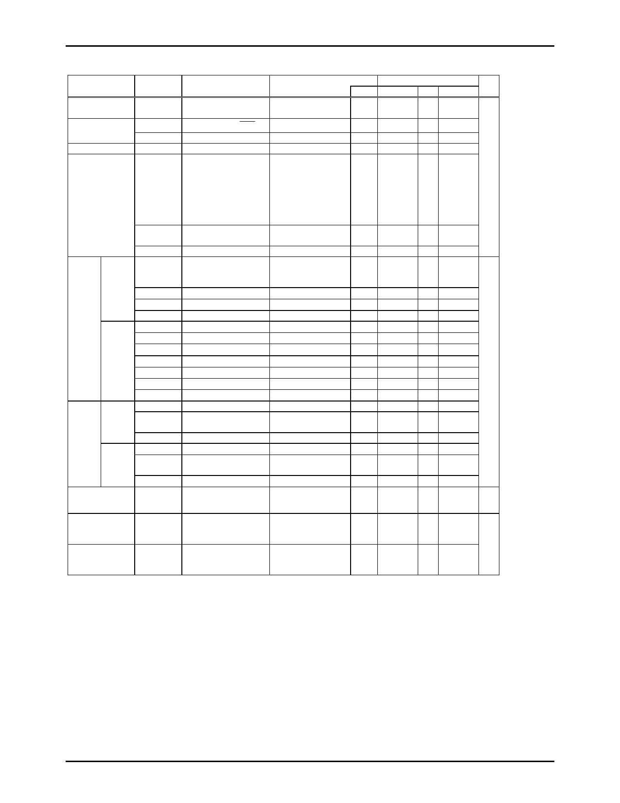
1. Absolute Maximum Ratings at Ta=25°C and VSS1=VSS2=0V
Parameter
Symbol
Pins
Supply voltage
Input voltage
Output voltage
Input/Output
voltage
High
level
output
current
Peak
output
current
Total
output
current
Low
level
output
current
Peak
output
current
Total
output
current
Maximum power
dissipation
VDDMAX
VI(1)
VI(2)
VO(1)
VIO(1)
VIO(2)
VIO(3)
IOPH(1)
IOPH(2)
IOPH(3)
IOPH(4)
ΣIOAH(1)
ΣIOAH(2)
ΣIOAH(3)
ΣIOAH(4)
ΣIOAH(5)
ΣIOAH(6)
ΣIOAH(7)
IOPL(1)
IOPL(2)
IOPL(3)
ΣIOAL(1)
ΣIOAL(2)
ΣIOAL(3)
Pdmax
VDD1,VDD2,
VDD3,VDD4
XT1,XT2,CF1, RES
VP
S0/T0 to S15/T15
•Port 0: CMOS output
option
•Port 1
•Port 3: CMOS output
option
•Port 7
•Port 8
•Port 0 open drain
•Port 3 open drain
S16 to S51
Port 0, 1, 3
Port71,72,73
S0/T0 to S15/T15
S16 to S51
Port 0
Port 1,3
Port 7
S0/T0 to S15/T15
S16 to S27
S28 to S39
S40 to S51
Port 02,03
•Port 00,01,04 to 07
•Port 1,3
Port 7,8
Port 00,01,02,03
•Port 04,05,06,07
•Port 1,3
Ports 7,8
QIP100E
Operating
Topr
temperature
range
Storage
Tstg
temperature
range
Conditions
VDD1=VDD2=
VDD3=VDD4
Ratings
unit
VDD[V] min. typ. max.
-0.3
+7.0 V
-0.3
VDD-45
VDD-45
-0.3
VDD+0.3
VDD+0.3
VDD+0.3
VDD+0.3
•CMOS output
selected
•Current at each pin
Current at each pin
Current at each pin
Current at each pin
Total of all pins
Total of all pins
Total of all pins
Total of all pins
Total of all pins
Total of all pins
Total of all pins
For each pin
For each pin
For each pin
For each pin
For each pin
For each pin
Ta = -30 to+70°C
-0.3
VDD-45
-10
-3
-30
-15
-30
-30
-5
-65
-60
-60
-60
-30
-55
15
VDD+0.3
mA
30
20
5
60
50
20
mW
70 °C
125
No.6843-10/23
Share Link: 