CXA2596M View Datasheet(PDF) - Sony Semiconductor
Part Name
Description
Manufacturer
CXA2596M Datasheet PDF : 17 Pages
| |||
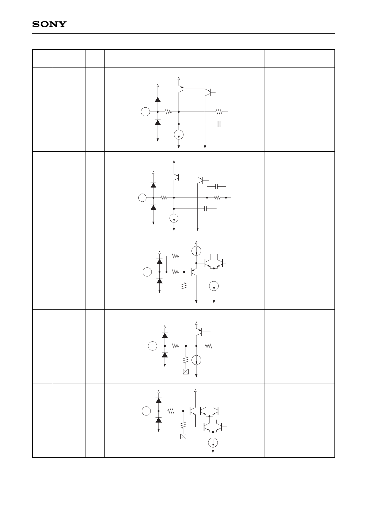
Pin
Symbol IO
No.
13
TE
O
14
FE
O
15
RFE
—
16
RFO
O
Equivalent circuit
VCC
147
13
158.45k
400µ
VEE
VCC
10p
VEE
25p
147
87k
14
400µ
VEE
10p
VEE
25.4k
25µ
5.7k
15
5k
VCC
147
16
60k
25.4k
800µ
CXA2596M
Description
Output pin of tracking
error amplifier.
The F-E signal is
output.
Output pin of focus
error amplifier.
Equalizing pin of RF
amplifier.
Frequency response
can be adjusted by
connecting CR to this
pin.
Output pin of RF
amplifier.
17
RF_I
I
147
17
15k
20µ
—5—
Input pin of RF amplifier
output RFO with
capacitance coupled.
Share Link: 