MAX038EVKIT View Datasheet(PDF) - Maxim Integrated
Part Name
Description
Manufacturer
MAX038EVKIT Datasheet PDF : 8 Pages
| |||
MAX038 Evaluation Kit
JU3 to allow the frequency to be adjusted. Verify
that there is a shunt on JU5.
4) Verify the shunts on JU1 and JU2 for a square-wave
output. Refer to Table 1 for alternate waveform
selections.
5) Apply power and verify the output waveform.
_______________Detailed Description
Waveform Selection
To select the desired output waveform, place shunts
across JU1 and JU2 in the combinations shown in
Table 1. These jumpers set address pins A0 and A1 to
TTL/CMOS-logic levels. External control may be initiat-
ed by connecting an external source to the A0 and
A1 pads and removing the shunts on JU1 and JU2.
Note that there are 10kΩ pull-up resistors to +5V on the
A0 and A1 address lines.
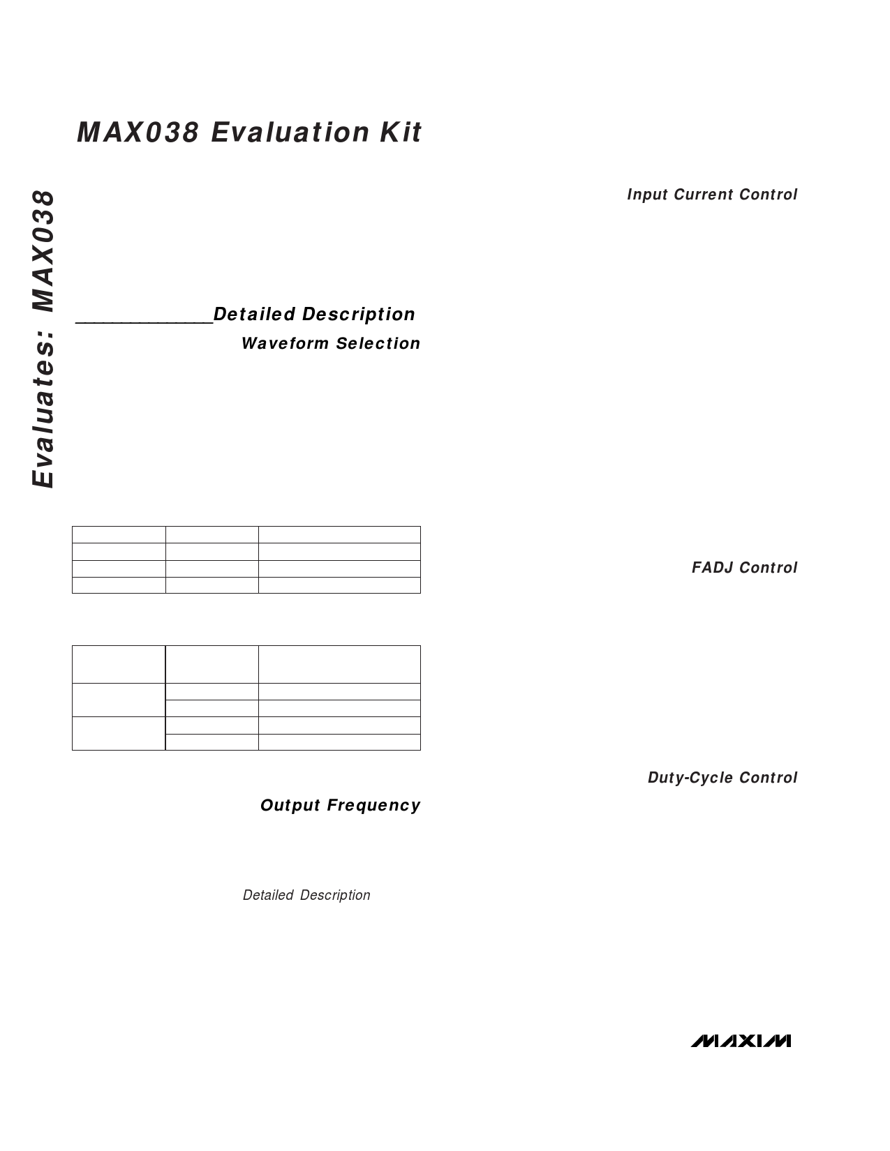
Table 1. Waveform Jumper Select
JU1
Don't Care
Open
Short
JU2
Open
Short
Short
OUTPUT WAVEFORM
Sine Wave
Triangle Wave
Square Wave
Table 2. Frequency and Duty-Cycle Jumper Select
JUMPER
JU3
JU4
SHUNT
LOCATION
1&2
2&3
1&2
2&3
MAX038 OUTPUT
Adjustable Frequency
Pre-Set Frequency*
Adjustable Duty Cycle
Fixed 50% Duty Cycle
* Note: Frequency pre-set by oscillator capacitor (C1) and input
current (position of R3) as specified by formula [1].
Output Frequency
The output frequency is controlled by the oscillator
capacitor (C1), the current injected into the IIN pin, and
the voltage on the FADJ pin. The EV kit allows indepen-
dent adjustment of both input current (R3) and FADJ
voltage (R2). Refer to the Detailed Description section
of the MAX038 data sheet for additional theory of oper-
ation.
Input Current Control
The current injected into the IIN pin acts as the primary
frequency-adjustment control. The R3 potentiometer
varies the current to the MAX038’s IIN pin. The input
current can be easily monitored by removing the JU5
shunt and placing a current meter across the JU5 pins.
The components supplied on the EV kit will allow an
input current range of 50µA to 725µA. With the VADJ
pin grounded, the fundamental output frequency (Fo) is
as follows:
Fo (MHz) = IIN(µA) ÷ COSC (pF)
[1]
where: IIN = current injected into IIN
= VREF ÷ (R3 + R12)
= 2.5V ÷ (0kΩ to 50kΩ + 3.3kΩ)
COSC = external oscillator capacitor (C1)
To use an external input current, connect the external
current source to the IIN pad and remove the JU5 shunt
completely. Note that there is a 3.3kΩ resistor in series
with the device IIN pin.
FADJ Control
Varying the FADJ voltage will also vary the output fre-
quency. With a shunt across pins 1 and 2 of JU3, the
R2 potentiometer will vary the voltage applied to the
FADJ pin. With the JU3 shunt on pins 2 and 3, the FADJ
pin is grounded. Grounding the FADJ pin sets the out-
put to the fundamental output frequency (Fo), as
given by equation [1].
To use an external FADJ voltage, connect the external
source to the FADJ pad and remove the JU3 shunt
completely. Limit the external FADJ voltage to ±2.4V.
Duty-Cycle Control
The voltage on the DADJ pin controls the duty cycle of
the output waveform. With the JU4 shunt on pins 1 and 2,
the R1 potentiometer will vary the voltage applied to the
DADJ pin, thus varying the duty cycle 15% to 85%. With
the JU4 shunt on pins 2 and 3, the DADJ pin is grounded.
Grounding the DADJ pin fixes the duty cycle at 50%.
To use an external DADJ voltage, connect the external
voltage source to the DADJ pad and remove the JU4
shunt completely. Limit the external DADJ voltage to
±2.3V.
2 _______________________________________________________________________________________
Share Link: 