CXD2529Q View Datasheet(PDF) - Sony Semiconductor
Part Name
Description
Manufacturer
CXD2529Q Datasheet PDF : 64 Pages
| |||
CXD2529Q
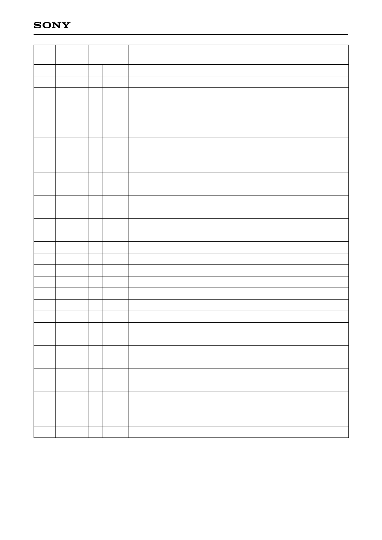
Pin
No.
Symbol
I/O
Description
70 C4M
O 1, 0 4.2336MHz output. 1/4 frequency-divided VCKI output in CAV-W mode.
71 DOUT O 1, 0 Digital Out output.
72 EMPH
O
1, 0
Outputs a high signal when the playback disc has emphasis, and a low
signal when there is no emphasis.
73 EMPHI I
Inputs a high signal when de-emphasis is on, and a low signal when de-
emphasis is off.
74 WFCK O 1, 0 WFCK output.
75 SCOR O 1, 0 Outputs a high signal when either subcode sync S0 or S1 is detected.
76 SBSO O 1, 0 Sub P to W serial output.
77 EXCK
I
SBSO readout clock input.
78 VSS
— — GND.
79 VDD
— — Power supply (+5V).
80 SYSM
I
Mute input. Active when high.
81 NC
82 AVSS
— — Analog GND.
83 AVDD
— — Analog power supply (+5V).
84 AOUT1 O
Left-channel analog output.
85 AIN1
I
Left-channel operational amplifier input.
86 LOUT1 O
Left-channel LINE output.
87 AVSS
— — Analog GND.
88 XVDD
Power supply for master clock.
89 XTAI
I
Crystal oscillation circuit input. Input the external master clock via this pin.
90 XTAO
O
Crystal oscillation circuit output.
91 XVSS
GND for master clock.
92 AVSS
— — Analog GND.
93 LOUT2 O
Right-channel LINE output.
94 AIN2
I
Right-channel operational amplifier input.
95 AOUT2 O
Right-channel analog output.
96 AVDD
— — Analog power supply (+5V).
97 AVSS
— — Analog GND.
98 NC
99 NC
100 XRST
I
System reset. Reset when low.
Notes) • PCMD is an MSB first, two’s complement output.
• GTOP is used to monitor the frame sync protection status. (High: sync protection window released.)
• XUGF is the negative pulse for the frame sync derived from the EFM signal. It is the signal before
sync protection.
• XPLCK is the inverse of the EFM PLL clock. The PLL is designed so that the falling edge of XPLCK
and the EFM signal transition point coincide.
• GFS goes high when the frame sync and the insertion protection timing match.
• RFCK is derived with the crystal accuracy. This signal has a cycle of 136µs (during normal-speed).
• C2PO represents the data error status.
• XRAOF is generated when the 16K RAM exceeds the ±4F jitter margin.
–6–
Share Link: 