CXD2529Q View Datasheet(PDF) - Sony Semiconductor
Part Name
Description
Manufacturer
CXD2529Q Datasheet PDF : 64 Pages
| |||
CXD2529Q
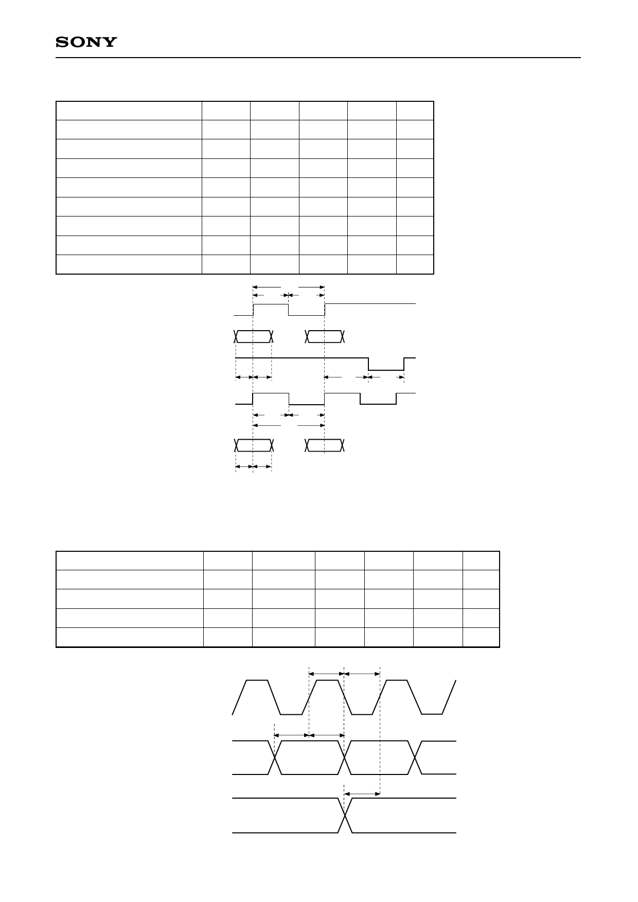
2. CLOK, DATA, XLAT, CNIN, SQCK and EXCK pins (VDD = AVDD = 5.0V ± 5%, VSS = AVSS = 0V, Topr = –20 to +75°C)
Item
Clock frequency
Clock pulse width
Setup time
Hold time
Delay time
Latch pulse width
EXCK SQCK frequency
EXCK SQCK pulse width
Symbol
fCK
tWCK
tSU
tH
tD
tWL
fT
fWT
Min.
750
300
300
300
750
750∗
Typ. Max. Unit
0.65 MHz
ns
ns
ns
ns
0.65∗
ns
MHz
ns
CLOK
1/fCK
tWCK
tWCK
DATA
XLAT
EXCK
CNIN
SQCK
SQSO
SBSO
tSU tH
tWT
tWT
1/fT
tSU tH
tD
tWL
∗ In pseudo double-speed playback mode, except when SQSO is Sub Q Read, the maximum operating
frequency for SQCK is 300kHz and the minimum pulse width is 1.5µs.
3. BCKI, LRCKI, PCMDI pins (VDD = AVDD = 5.0V ± 5%, VSS = AVSS = 0V, Topr = –20 to +75°C)
Item
BCK pulse width
DATAL, R setup time
DATAL, R hold time
LRCK setup time
Symbol Conditions Min.
tW
94
tSU
18
tH
18
tSU
18
Typ.
Max. Unit
ns
ns
ns
ns
tW (BCKI) tW (BCKI)
BCKI
VDD/2
VDD/2
tSU
tH
(PCMDI) (PCMDI)
PCMDI
tSU
(LRCKI)
LRCKI
–9–
Share Link: 