NT68275 View Datasheet(PDF) - Novatek Microelectronics
Part Name
Description
Manufacturer
NT68275 Datasheet PDF : 38 Pages
| |||
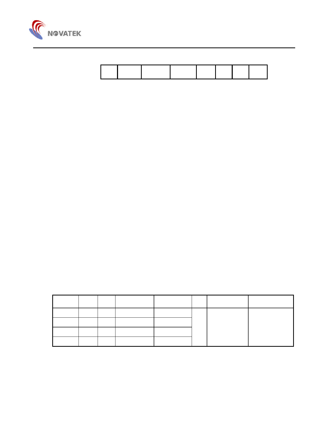
NT68275
7
6
5
4
3
2
1
0
Row 15
Column 18
RGBF FBKGOP
*PWM/INT
DBOUNCE
HPOL
VPOL VCO1
VCO0
OSD Screen Control 2
Bit 7: RGBF - This bit controls the driving state of output pins, R, G, B and FBKG when the OSD is disabled.
After power on, this bit is cleared to ‘0’ and all of the R, G, B and FBKG pins output a high impedance
state while the OSD is being disabled. If this bit is set to ‘1’, the R, G, B output pins will drive low, FBKG
pin drive high or low depend on FBKGOP (If FBKGOP=0, drive high. If FBKGOP=1, drive low) while OSD
being disabled.
Bit 6: FBKGOP - This bit selects the polarity of the output signal of FBKG pin. This signal is active low when the
user clears this bit. Otherwise, active high set this bit. Refer the figure 5 below for the FBKG output timing.
The default value is ‘1’ after power on.
Bit 5: * PWM/INT - This bit selects the output option to PWM/INT pin. This bit will enable the PWM clock output
as it is set to ‘1’. Otherwise, it will select the INT option. Refer the figure 5 bellow for the INT output timing.
The default value is ‘0’ after power on.
Bit 4: DBOUNCE - This bit is to activate the debounce circuit of horizontal and vertical scan. It is to prevent from
the OSD screen shaking when user adjusts the horizontal phase or vertical position. This bit will be
cleared after power on.
Bit 3: HPOL - This bit selects the polarity of the input signal of horizontal sync (HFLB pin). If the input sync signal
is negative polarity, user must clear this bit. Otherwise, set this bit to ‘1’ to accept the positive polarity
signal. After power on, this bit is cleared to ‘0’ and it will accept negative polarity sync signal.
Bit 2: VPOL - This bit selects the polarity of the input signal of vertical sync ( VFLB pin). If the input sync signal is
negative polarity, user must clear this bit. Otherwise, set this bit to ‘1’ to accept the positive polarity signal.
After power on, this bit is cleared to ‘0’ and it will accept negative polarity sync signal.
Bit 1-0: VCO1/0 – These bits select the VCO frequency range when user set the horizontal display resolution
flexibly. It is related to the horizontal display resolution and user must set the control register at row15 /
column15 properly. The default value is VCO1=0 & VCO0=0 after power on state. The relationship
between VCO1/0 and display resolution is list below:
TAB 6. P.R. (Pixel Rate) = HDR * 12 * FreqHFLB
Section VCO1 VCO0 VCO Freq. Min VCO Freq. Max Unit
P.R. Limit
HFLB Freq. Limit
Freq1
0
0
*6
Freq2
0
1
*14
Freq3
1
0
*29
Freq4
1
1
*61
*13
*28
*60
*120
MHz Min < P.R. < Max
(Min / HDR*12) <
FreqHFLB
< Max / (HDR*12)
If there are no signals at HFLB input, the PLL will generate an approximate 2.5 MHz clock to ensure the proper
operation of the IIC bus and other control registers.
19
Share Link: 