XR-T5684 View Datasheet(PDF) - Exar Corporation
Part Name
Description
Manufacturer
XR-T5684 Datasheet PDF : 16 Pages
| |||
XR-T5684
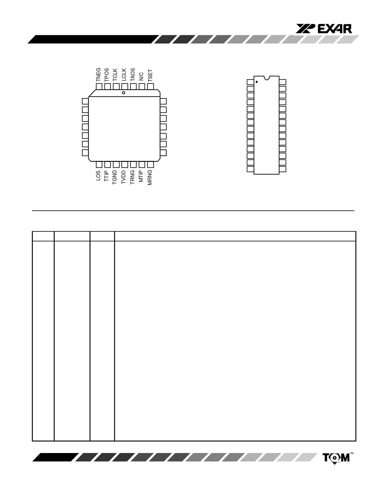
PIN CONFIGURATION
4 3 2 1 28 27 26
MODE 5
RPOS 6
RNEG 7
RCLK 8
PD 9
CLKDS 10
DPM 11
25 LEN2
24 LEN1
23 LEN0
22 RGND
21 RVDD
20 RRING
19 RTIP
12 13 14 15 16 17 18
28 Lead PLCC
LCLK 1
TCLK 2
TPOS 3
TNEG 4
MODE 5
RPOS 6
RNEG 7
RCLK 8
PD 9
CLKDS 10
DPM 11
LOS 12
TTIP 13
TGND 14
28 TAOS
27 N/C
26 TEST
25 LEN2
24 LEN1
23 LEN0
22 RGND
21 RVDD
20 RRING
19 RTIP
18 MRING
17 MTIP
16 TRING
15 TVDD
28 Lead PDIP (0.600”)
PIN DESCRIPTION
Pin #
1
Symbol
LCLK
2
TCLK
3
TPOS
4
TNEG
5
MODE
6
RPOS
7
RNEG
8
RCLK
9
PD
10
CLKDS
11
DPM
Type
I
I
I
I
I
O
O
O
I
I
O
Description
Oversampling Clock. 8X or 16X input clock for receive clock recovery circuit.
8X=12.352MHz±200ppm with pin 9 set to low. 16X=24.704MHz ±200ppm with pin 9 set to high.
Transmit Clock. T1=1.544MHz±50ppm.
Transmit Positive Data. A positive NRZ data on this pin causes a positive pulse to be trans-
mitted on TTIP. TPOS is sampled on the falling edge of TCLK.
Transmit Negative Data. A positive NRZ data on this pin causes a negative pulse to be
transmitted on TRING. TNEG is sampled on the falling edge of TCLK.
Receive Output Data Select. With this pin set to high, the extracted data at RPOS and
RNEG are re-timed using the recovered clock RCLK. With this pin set to low, the received
data have no relation to RCLK and are typically stretched by 80nS before being sent to the
output. This pin is pulled down internally.
Receive Positive Data Output. A positive pulse on this pin corresponds to a positive pulse
on RTIP.
Receive Negative Data Output. A positive pulse on this pin corresponds to a positive pulse
on RRING.
Receive Clock Output. Recovered clock using oversampling clock applied to pin 1. See
MODE select of pin 5 and PD of pin 9.
Programmable Divider. The state of this pin determines the oversampling clock applied to
pin 1. When LCLK=16X1.544MHz, set PD to high. When LCLK=8X1.544MHz, set PD to low.
This pin is pulled down internally.
Clock Disable. With this pin set to high, the recovered clock at pin 8 is disabled. This func-
tion is provided for applications where upon input data loss, the output clock can be inhibited
by connecting LOS to CLKDS externally. This pin is pulled down internally.
Driver Performance Monitor. Used as an early warning signal on non-functioning T1 links. If
no signal is present on MTIP and MRING for 63 clock cycles. DPM goes high until a next
pulse is detected.
Rev 1.01
4
Share Link: 