XR-T5684 View Datasheet(PDF) - Exar Corporation
Part Name
Description
Manufacturer
XR-T5684 Datasheet PDF : 16 Pages
| |||
XR-T5684
SYSTEM DESCRIPTION
The device consists of receiver and transmitter circuitry
with separate power supplies to reduce crosstalk
between the two sections.
RECEIVER
The receiver is sensitive to the entire cable length from
the cross-connect and requires no external equalization
networks. The receive AMI input signal is applied to RTIP
and RRING through a center-grounded transformer. The
positive pulse is input to RTIP and the negative pulse is
input to RRING.
Comparators are used to slice the data on RTIP and
RRING. The slicing level of the comparators are
dynamically set at around 70% of peak level of the input
signal to ensure optimum signal-to-noise ratio. With Mode
Select (pin 5) set to low, the clock recovery feature is
bypassed and the output data from the comparators are
typically stretched by 80nS before output to RPOS and
RNEG respectively.
A positive data at RPOS corresponds to a positive pulse
received at RTIP and a positive data at RNEG
corresponds to a positive pulse received at RRING.
With Mode Select (pin 5) set to high and an oversampling
clock applied to pin 1, the recovered data can be
synchronized with RCLK at pin 8. The clock recovery circuit
extracts the timing contents from the incoming data
transitions by means of an 8X or 16X divider. If there is no
data on the input, the divider operates in its free running
mode, generating a equal mark-and-space ratio output
clock. This free running mode will be interrupted if a positive
pulse is detected; the resultant mark-and-space ratio of the
output clock is then determined by the position of the
occurrence of the positive data relative to its free running
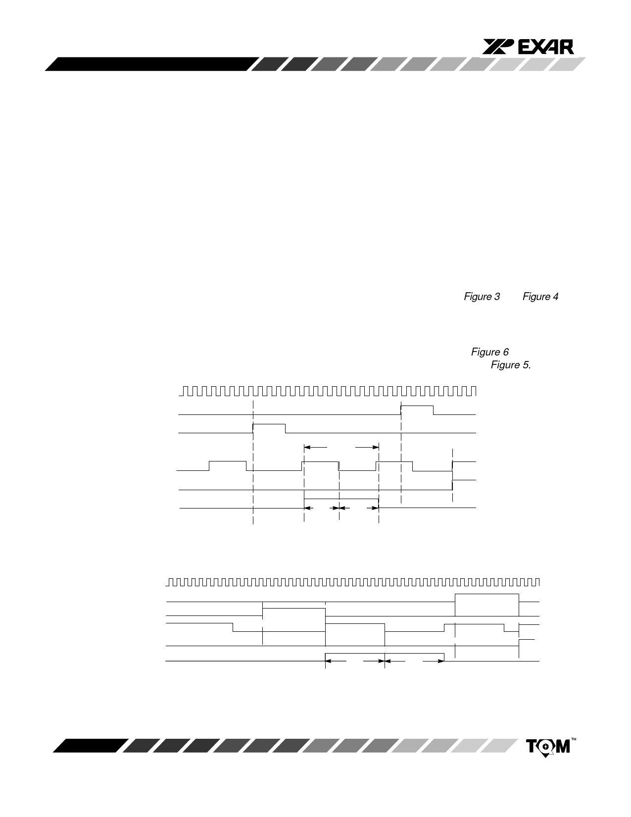
position. See timing diagram in Figure 3 and Figure 4.
In all cases, the output data RPOS and RNEG remains
stable on the falling edge of RCLK so as to be sampled
correctly. The input jitter tolerance with an 8X
oversampling clock is shown in Figure 6 and that with a
16X oversampling clock is shown in Figure 5.
8X OVERSAMPLING
RTIP
RRING
648nS
RCLK
RPOS
RNEG
tsu
tho
6 Clk Cycles
6 Clk Cycles
Figure 3. Receiver Clock and Data Switching Characteristics
16 X OVERSAMPLING
RTIP
RRING
RCLK
RPOS
RNEG
8 Clk Cycles
tsu
8 Clk Cycles
tho
Figure 4. Typical Receive Timing Diagram Using 8X Oversampling Clock.
Rev 1.01
8
Share Link: 