6N139 View Datasheet(PDF) - Sharp Electronics
Part Name
Description
Manufacturer
6N139 Datasheet PDF : 5 Pages
| |||
6N139
s Electro-optical Characteristics
( Ta = 0 to + 70˚C unless otherwise specified )
Parameter
Symbol
Conditions
MIN. TYP. MAX. Unit
*1Current transfer ratio
Logic ( 0) output voltage
CTR(1) IF = 0.5mA, VO = 0.4V, V CC = 4.5V
400 1 800
-
%
CTR(2) IF = 1.6mA, VO = 0.4V, V CC = 4.5V
500 1 600
-
%
V OL(1) IO = 6.4mA, VCC = 4.5V, I F= 1.6mA
-
0.1
0.4
V
V OL(2) IO = 15mA, VCC = 4.5V, I F = 5mA
-
0.1
0.4
V
V OL(2) IO = 24mA, V CC = 4.5V, I F = 12mA -
0.1
0.4
V
Logic (1) output current
Logic ( 0) supply current
I OH IF = 0, V CC = V O = 18V
-
0.05 100
µA
ICCL IF = 1.6mA, V CC = 5V, V O = open
-
0.5
-
mA
Logic (1) supply current
I CCH IF = 0, V CC = 5V, V O = open
-
10
-
nA
Input forward voltage
V F IF = 1.6mA, Ta = 25˚C
-
1.5
1.7
V
Input forward voltage temperature coefficient
Input reverse voltage
*2 IF = 1.6mA
BVR IR = 10 µA, Ta = 25˚C
-
- 1.9
5.0
-
- mV/˚C
-
V
Input capacitance
CIN VF = 0, f = 1MHz
-
60
-
pF
*3Leak current (input-output )
*3Isolation resistance ( input-output )
*3Capacitance ( input-output )
I I-O
Ta = 25˚C, 45% RH, t = 5s
V I-O = 3kV DC
R I-O V I-O = 500V DC
CI-O f = 1MHz
-
-
1.0
µA
-
1012
-
Ω
-
0.6
-
pF
*1 Current transfer ratio is a ratio of input current
and output current expressed in % .
*2 ∆ VF/ ∆ Ta
*3 Measured as 2-pin element ( Short 1,2,3,4 and 5, 6, 7, 8. )
Note ) Typical value : at Ta = 25˚C, VCC = 5V
s Switching Characteristics
( Ta = 25˚C, VCC= 5V)
Parameter
*4Propagation delay time
Output (1) → ( 0)
*4Propagation delay time
Output ( 0) → (1)
**56Instantaneous common mode
rejection voltage “ Output (1)”
**56Instantaneous common mode
rejection voltage “ Output ( 0) ”
Symbol
t PHL
t PLH
CM H
CML
Conditions
RL = 4.7k Ω , I F = 0.5mA
RL = 270 Ω , I F = 12mA
RL = 4.7k Ω , I F = 0.5mA
RL = 270 Ω , I F = 12mA
IF = 0, VCM = 10V P-P
RL = 2.2k Ω
IF = 1.6 mA , VCM = 10V P-P
RL = 2.2k Ω
MIN.
-
-
-
-
-
TYP.
5
0.3
10
1.5
500
MAX.
25
1
60
7
-
Unit
µs
µs
µs
µs
V/ µ s
-
- 500
-
V/ µ s
*5 Instantaneous common mode rejection voltage “ output (1)” represents a common mode voltage variation that can hold the
output above (1) level ( VO > 2.0V).
*6 Instantaneous common mode rejection voltage “ output ( 0) ” represents a common mode voltage variation that can hold the
output above ( 0) level ( VO < 0.8V).
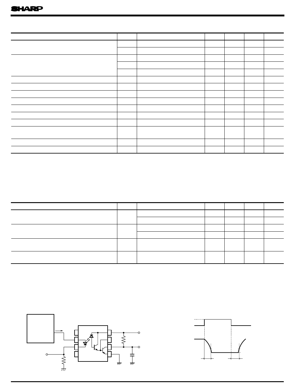
*4 Test circuit for Propagation Delay Time
Pulse input
duty ratio
= 1/10
Pulse generator
IF
1
2
3
IF monitor
4
100 Ω
8
VCC
7
RL
6
VO
5
CL = 15pF
IF
0
VO
5V
1.5V
1.5V
VOL
tPHL
tPLH
Share Link: 