LT1963EQ View Datasheet(PDF) - Linear Integrated System
Part Name
Description
Manufacturer
LT1963EQ Datasheet PDF : 16 Pages
| |||
LT1963 Series
APPLICATIO S I FOR ATIO
Thermal Considerations
The power handling capability of the device is limited by the
maximum rated junction temperature (125°C). The power
dissipated by the device is made up of two components:
1. Output current multiplied by the input/output voltage
differential: (IOUT)(VIN – VOUT), and
2. GND pin current multiplied by the input voltage:
(IGND)(VIN).
The GND pin current can be found using the GND Pin
Current curves in the Typical Performance Characteris-
tics. Power dissipation will be equal to the sum of the two
components listed above.
The LT1963 series regulators have internal thermal lim-
iting designed to protect the device during overload
conditions. For continuous normal conditions, the maxi-
mum junction temperature rating of 125°C must not be
exceeded. It is important to give careful consideration to
all sources of thermal resistance from junction to ambi-
ent. Additional heat sources mounted nearby must also
be considered.
For surface mount devices, heat sinking is accomplished
by using the heat spreading capabilities of the PC board
and its copper traces. Copper board stiffeners and plated
through-holes can also be used to spread the heat gener-
ated by power devices.
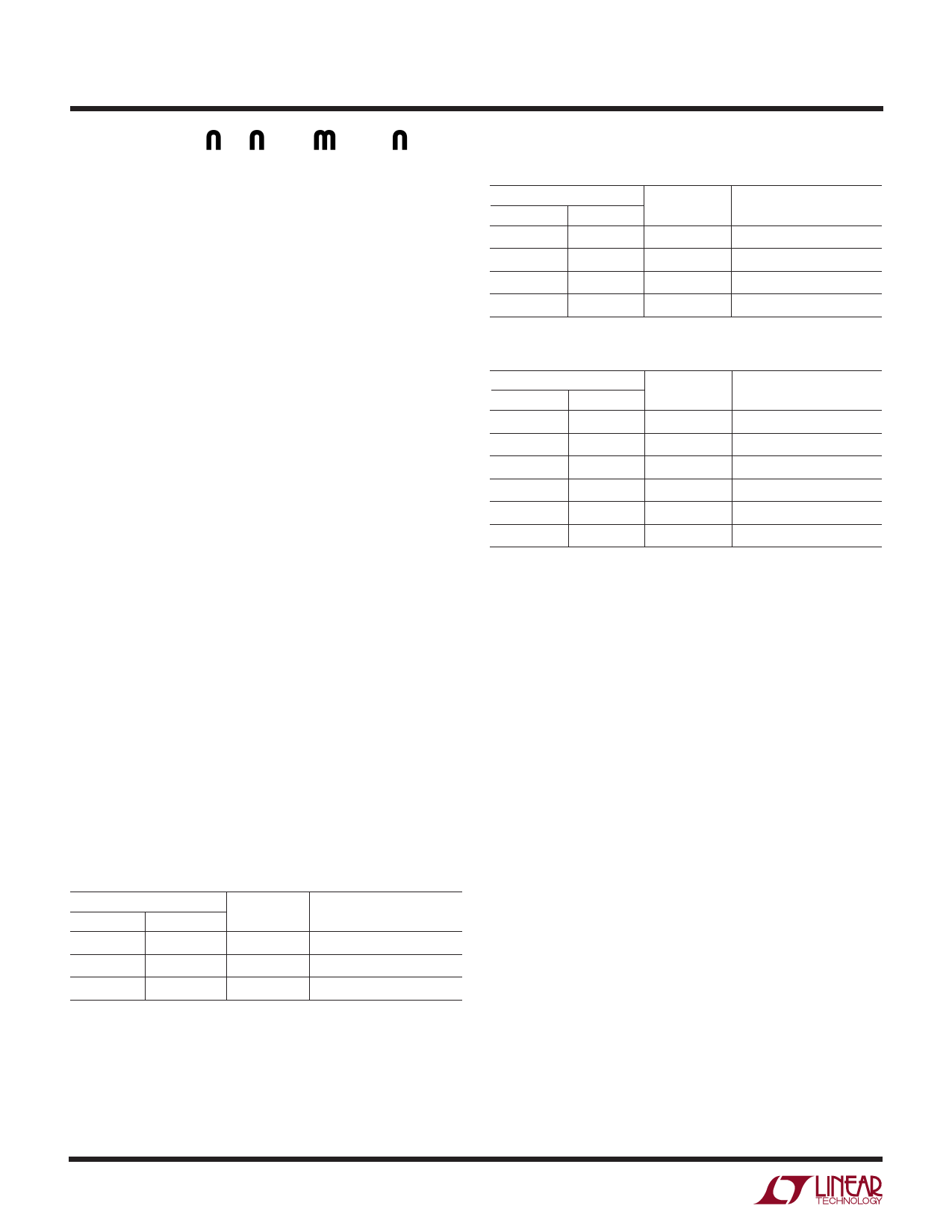
The following tables list thermal resistance for several
different board sizes and copper areas. All measurements
were taken in still air on 1/16" FR-4 board with one ounce
copper.
Table 1. Q Package, 5-Lead DD
COPPER AREA
TOPSIDE* BACKSIDE
2500mm2 2500mm2
BOARD AREA
2500mm2
1000mm2 2500mm2 2500mm2
125mm2 2500mm2 2500mm2
*Device is mounted on topside
THERMAL RESISTANCE
(JUNCTION-TO-AMBIENT)
23°C/ W
25°C/ W
33°C/ W
Table 2. SO-8 Package, 8-Lead SO
COPPER AREA
TOPSIDE* BACKSIDE
2500mm2 2500mm2
BOARD AREA
2500mm2
1000mm2 2500mm2 2500mm2
225mm2 2500mm2 2500mm2
100mm2 2500mm2 2500mm2
*Device is mounted on topside.
THERMAL RESISTANCE
(JUNCTION-TO-AMBIENT)
55°C/ W
55°C/ W
63°C/ W
69°C/ W
Table 3. SOT-223 Package, 3-Lead SOT-223
COPPER AREA
TOPSIDE* BACKSIDE
2500mm2 2500mm2
BOARD AREA
2500mm2
THERMAL RESISTANCE
(JUNCTION-TO-AMBIENT)
42°C/ W
1000mm2 2500mm2 2500mm2
42°C/ W
225mm2 2500mm2 2500mm2
50°C/ W
100mm2 2500mm2 2500mm2
56°C/ W
1000mm2 1000mm2 1000mm2
49°C/ W
1000mm2
0mm2
1000mm2
52°C/ W
*Device is mounted on topside.
T Package, 5-Lead TO-220
Thermal Resistance (Junction-to-Case) = 4°C/W
Calculating Junction Temperature
Example: Given an output voltage of 3.3V, an input voltage
range of 4V to 6V, an output current range of 0mA to
500mA and a maximum ambient temperature of 50°C,
what will the maximum junction temperature be?
The power dissipated by the device will be equal to:
IOUT(MAX)(VIN(MAX) – VOUT) + IGND(VIN(MAX))
where,
IOUT(MAX) = 500mA
VIN(MAX) = 6V
IGND at (IOUT = 500mA, VIN = 6V) = 10mA
So,
P = 500mA(6V – 3.3V) + 10mA(6V) = 1.41W
Using a DD package, the thermal resistance will be in the
range of 23°C/W to 33°C/W depending on the copper
area. So the junction temperature rise above ambient will
be approximately equal to:
1.41W(28°C/W) = 39.5°C
1963fa
12
Share Link: 