UPD78F0034BYGC(A)-8BS View Datasheet(PDF) - NEC => Renesas Technology
Part Name
Description
Manufacturer
UPD78F0034BYGC(A)-8BS Datasheet PDF : 90 Pages
| |||
µPD78F0034B, 78F0034BY, 78F0034B(A), 78F0034BY(A)
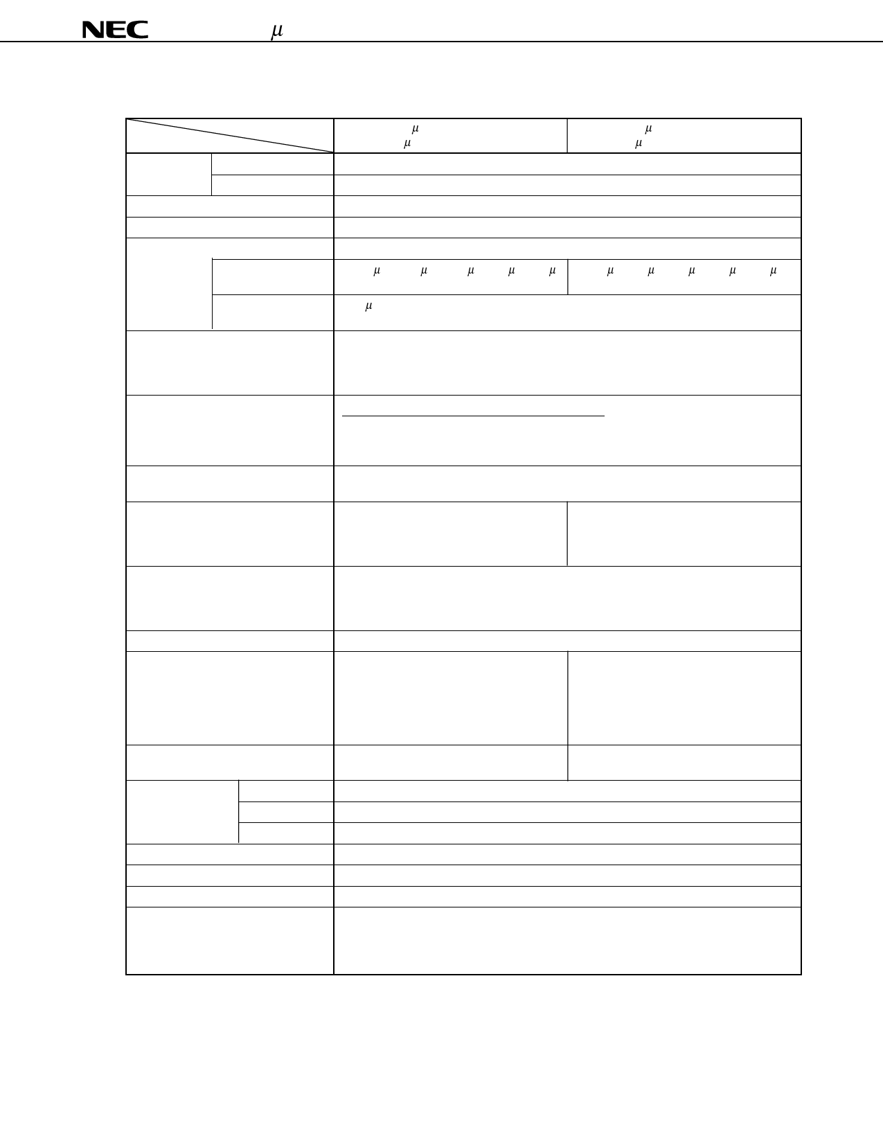
OVERVIEW OF FUNCTIONS
Item
Part Number
Internal
memory
Flash memory
High-speed RAM
Memory space
General-purpose registers
Minimum instruction execution time
When main system
When subsystem
clock selected
Instruction set
I/O ports
A/D converter
Serial interface
Timers
Timer outputs
Clock output
Buzzer output
Vectored interrupt Maskable
sources
Non-maskable
Software
Test inputs
Supply voltage
Operating ambient temperature
Package
µPD78F0034B
µPD78F0034B(A)
32 KBNote 1
1,024 bytesNote 1
µPD78F0034BY
µPD78F0034BY(A)
64 KB
8 bits × 32 registers (8 bits × 8 registers × 4 banks)
On-chip minimum instruction execution time cycle variable function
0.166 µs/0.333 µs/0.666 µs/1.33 µs/2.66 µs 0.238 µs/0.48 µs/0.95 µs/1.91 µs/3.81 µs
(@ 12 MHz operation, VDD = 4.5 to 5.5 V) (@ 8.38 MHz operation, VDD = 4.0 to 5.5 V)
122 µs (@ 32.768 kHz operation)
• 16-bit operation
• Multiply/divide (8 bits × 8 bits, 16 bits ÷ 8 bits)
• Bit manipulation (set, reset, test, Boolean operation)
• BCD adjust, etc.
Total:
51
• CMOS input:
8
• CMOS I/O:
39
• N-ch open-drain I/O (5 V withstand voltage): 4
• 10-bit resolution × 8 channels
• Operable over a wide power supply voltage range: AVDD = 1.8 to 5.5 V
• UART mode:
1 channel
• 3-wire serial I/O mode: 2 channels
• UART mode:
1 channel
• 3-wire serial I/O mode: 1 channel
• I2C bus mode
(multimaster supporting): 1 channel
• 16-bit timer/event counter: 1 channel
• 8-bit timer/event counter: 2 channels
• Watch timer:
1 channel
• Watchdog timer:
1 channel
3 (8-bit PWM output capable: 2)
• 93.75 kHz, 187.5 kHz, 375 kHz, 750 kHz,
1.25 MHz, 3 MHz, 6 MHz, 12 MHz
(@ 12 MHz operation with main system
clock)
• 32.768 kHz (@ 32.768 kHz operation with
subsystem clock)
• 65.5 kHz, 131 kHz, 262 kHz, 524 kHz, 1.05
MHz, 2.10 MHz, 4.19 MHz, 8.38 MHz
(@ 8.38 MHz operation with main system
clock)
• 32.768 kHz (@ 32.768 kHz operation with
subsystem clock)
1.46 kHz, 2.93 kHz, 5.86 kHz, 11.7 kHz
1.02 kHz, 2.05 kHz, 4.10 kHz, 8.19 kHz
(@ 12 MHz operation with main system clock) (@ 8.38 MHz operation with main system clock)
Internal: 13, external: 5
Internal: 1
1
Internal: 1, external: 1
VDD = 1.8 to 5.5 V
TA = –40 to +85°C
• 64-pin plastic LQFP (10 x 10)
• 64-pin plastic LQFP (14 x 14)
• 64-pin plastic TQFP (12 x 12)
• 73-pin plastic FBGA (9 x 9)Note 2
Notes 1.
2.
The capacities of the flash memory and the internal high-speed RAM can be changed with the memory
size switching register (IMS).
The special grade version of the 73-pin plastic FBGA (9 x 9) is not provided.
Data Sheet U16369EJ1V0DS
7
Share Link: 