KL27P64M48SF6 View Datasheet(PDF) - Freescale Semiconductor
Part Name
Description
Manufacturer
KL27P64M48SF6 Datasheet PDF : 64 Pages
| |||
General
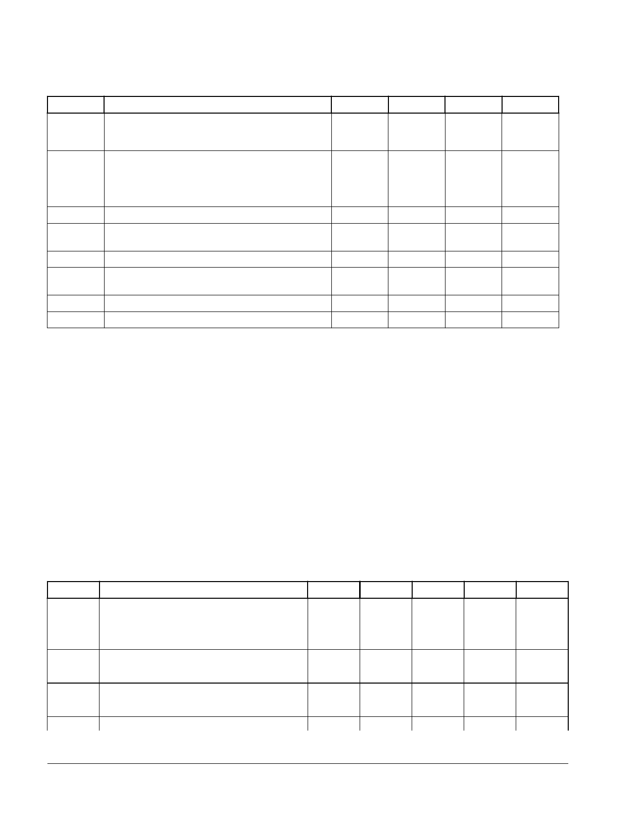
Table 7. Voltage and current operating behaviors (continued)
Symbol
Description
• 2.7 V ≤ VDD ≤ 3.6 V, IOL = 5 mA
• 1.71 V ≤ VDD ≤ 2.7 V, IOL = 1.5 mA
Min.
Max.
Unit
—
0.5
V
VOL
Output low voltage — High drive pad
• 2.7 V ≤ VDD ≤ 3.6 V, IOL = 18 mA
• 1.71 V ≤ VDD ≤ 2.7 V, IOL = 6 mA
—
0.5
V
—
0.5
V
IOLT
Output low current total for all ports
—
IIN
Input leakage current (per pin) for full temperature
—
range
100
mA
1
μA
IIN
Input leakage current (per pin) at 25 °C
IIN
Input leakage current (total all pins) for full
temperature range
—
0.025
μA
—
μA
IOZ
Hi-Z (off-state) leakage current (per pin)
RPU
Internal pullup resistors
—
1
μA
20
50
kΩ
Notes
1
2
2
2
3
1. PTB0, PTB1, PTC3, PTC4, PTD6, and PTD7 I/O have both high drive and normal drive capability selected by the
associated PTx_PCRn[DSE] control bit. All other GPIOs are normal drive only.
2. Measured at VDD = 3.6 V
3. Measured at VDD supply voltage = VDD min and Vinput = VSS
2.2.4 Power mode transition operating behaviors
All specifications except tPOR and VLLSx→RUN recovery times in the following table
assume this clock configuration:
• CPU and system clocks = 48 MHz
• Bus and flash clock = 24 MHz
• HIRC clock mode
Table 8. Power mode transition operating behaviors
Symbol Description
Min.
Typ.
Max.
Unit
tPOR After a POR event, amount of time from the
—
point VDD reaches 1.8 V to execution of the first
instruction across the operating temperature
range of the chip.
—
300
μs
Notes
• VLLS0 → RUN
—
152
166
μs
• VLLS1 → RUN
—
152
166
μs
Table continues on the next page...
8
Freescale Semiconductor, Inc.
Kinetis KL27 With Up To 256 KB Flash, Rev3, 08/2014.
Share Link: 