S25FL127SABNFI101(2005) View Datasheet(PDF) - Cypress Semiconductor
Part Name
Description
Manufacturer
S25FL127SABNFI101 Datasheet PDF : 131 Pages
| |||
S25FL127S
128 Mbit (16 Mbyte)
3.0V SPI Flash Memory
Features
CMOS 3.0 Volt Core
Density
– 128 Mbits (16 Mbytes)
Serial Peripheral Interface (SPI) with Multi-I/O
– SPI Clock polarity and phase modes 0 and 3
– Extended Addressing: 24- or 32-bit address options
– Serial Command set and footprint compatible with S25FL-A,
S25FL-K, and S25FL-P SPI families
– Multi I/O Command set and footprint compatible with
S25FL-P SPI family
READ Commands
– Normal, Fast, Dual, Quad
– AutoBoot - power up or reset and execute a Normal or Quad read
command automatically at a preselected address
– Common Flash Interface (CFI) data for configuration information.
Programming (0.8 Mbytes/s)
– 256- or 512-byte Page Programming buffer options
– Quad-Input Page Programming (QPP) for slow clock systems
Erase (0.5 Mbytes/s)
– Hybrid sector size option - physical set of sixteen 4-kbyte sectors
at top or bottom of address space with all remaining sectors of
64 kbytes
– Uniform sector option - always erase 256-kbyte blocks for software
compatibility with higher density and future devices.
Performance Summary
Cycling Endurance
– 100,000 Program-Erase Cycles per sector minimum
Data Retention
– 20 Year Data Retention typical
Security features
– One Time Program (OTP) array of 1024 bytes
– Block Protection:
– Status Register bits to control protection against program or erase
of a contiguous range of sectors.
– Hardware and software control options
– Advanced Sector Protection (ASP)
– Individual sector protection controlled by boot code or password
Cypress® 65 nm MirrorBit Technology with Eclipse™ Architecture
Supply Voltage: 2.7V to 3.6V
Temperature Range:
– Industrial (-40°C to +85°C)
– Industrial Plus (-40°C to +105°C)
Packages (all Pb-free)
– 8-lead SOIC (208 mil)
– 16-lead SOIC (300 mil)
– 8-contact WSON 6 x 5 mm
– BGA-24 6 x 8 mm
– 5 x 5 ball (FAB024) and 4 x 6 ball (FAC024) footprint options
– Known Good Die and Known Tested Die
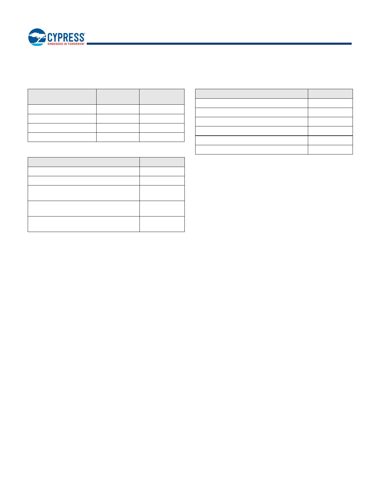
Maximum Read Rates
Command
Read
Fast Read
Dual Read
Quad Read
Clock Rate
(MHz)
50
108
108
108
Mbytes/s
6.25
13.5
27
54
Typical Program and Erase Rates
Operation
Page Programming (256-byte page buffer)
Page Programming (512-byte page buffer)
4-kbyte Physical Sector Erase (Hybrid Sector
Option)
64-kbyte Physical Sector Erase (Hybrid Sector
Option)
256-kbyte Logical Sector Erase (Uniform Sector
Option)
kbytes/s
650
800
30
500
500
Current Consumption
Operation
Serial Read 50 MHz
Serial Read 108 MHz
Quad Read 108 MHz
Program
Erase
Standby
Current (mA)
16 (max)
24 (max)
47 (max)
50 (max)
50 (max)
0.07 (typ)
Cypress Semiconductor Corporation • 198 Champion Court
Document Number: 001-98282 Rev. *F
• San Jose, CA 95134-1709 • 408-943-2600
Revised August 21, 2015
Share Link: 