S25FL127SABNFI101(2005) View Datasheet(PDF) - Cypress Semiconductor
Part Name
Description
Manufacturer
S25FL127SABNFI101 Datasheet PDF : 131 Pages
| |||
S25FL127S
5. Timing Specifications
5.1
Key to Switching Waveforms
Figure 5.1 Waveform Element Meanings
Input Valid at logic high or low High Impedance Any change permitted Logic high Logic low
Symbol
Output Valid at logic high or low High Impedance Changing, state unknown Logic high Logic low
Input Levels
VIO + 0.4V
0.7 x VCC
0.5 x VCC
Figure 5.2 Input, Output, and Timing Reference Levels
Timing Reference Level
0.2 x VCC
- 0.5V
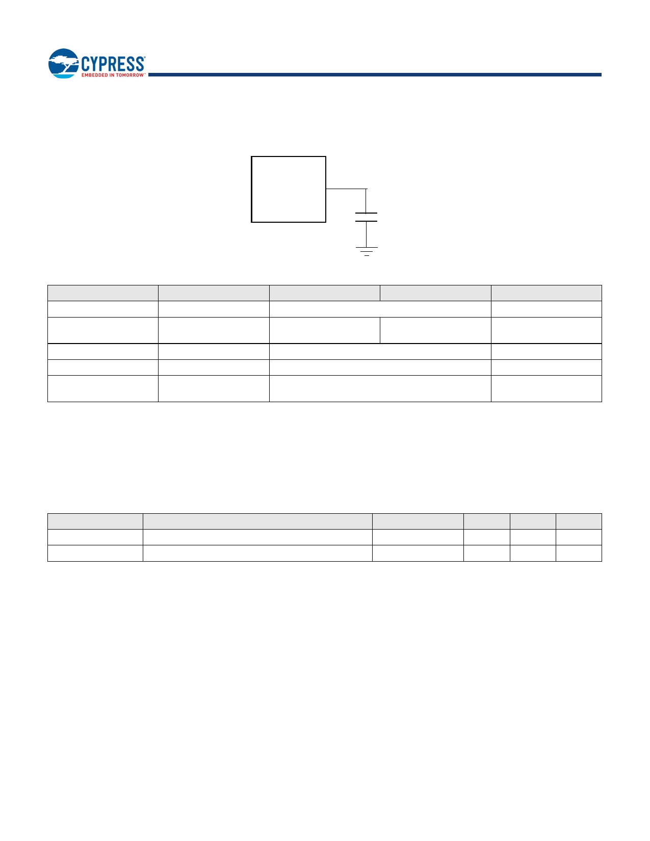
5.2 AC Test Conditions
Figure 5.3 Test Setup
Device
Under
Test
CL
Output Levels
0.85 x VCC
0.15 x VCC
Table 5.1 AC Measurement Conditions
Symbol
CL
Parameter
Load Capacitance
Input Rise and Fall Times
Input Pulse Voltage
Input Timing Ref Voltage
Output Timing Ref
Voltage
Min
Max
30
2.4
0.2 x VCC to 0.8 VCC
0.5 VCC
0.5 VCC
Notes:
1. Output High-Z is defined as the point where data is no longer driven.
2. Input slew rate: 1.5 V/ns.
3. AC characteristics tables assume clock and data signals have the same slew rate (slope).
Document Number: 001-98282 Rev. *F
Unit
pF
ns
V
V
V
Page 30 of 130
Share Link: 