TDA7550R_01 View Datasheet(PDF) - STMicroelectronics
Part Name
Description
Manufacturer
TDA7550R_01 Datasheet PDF : 10 Pages
| |||
TDA7550R
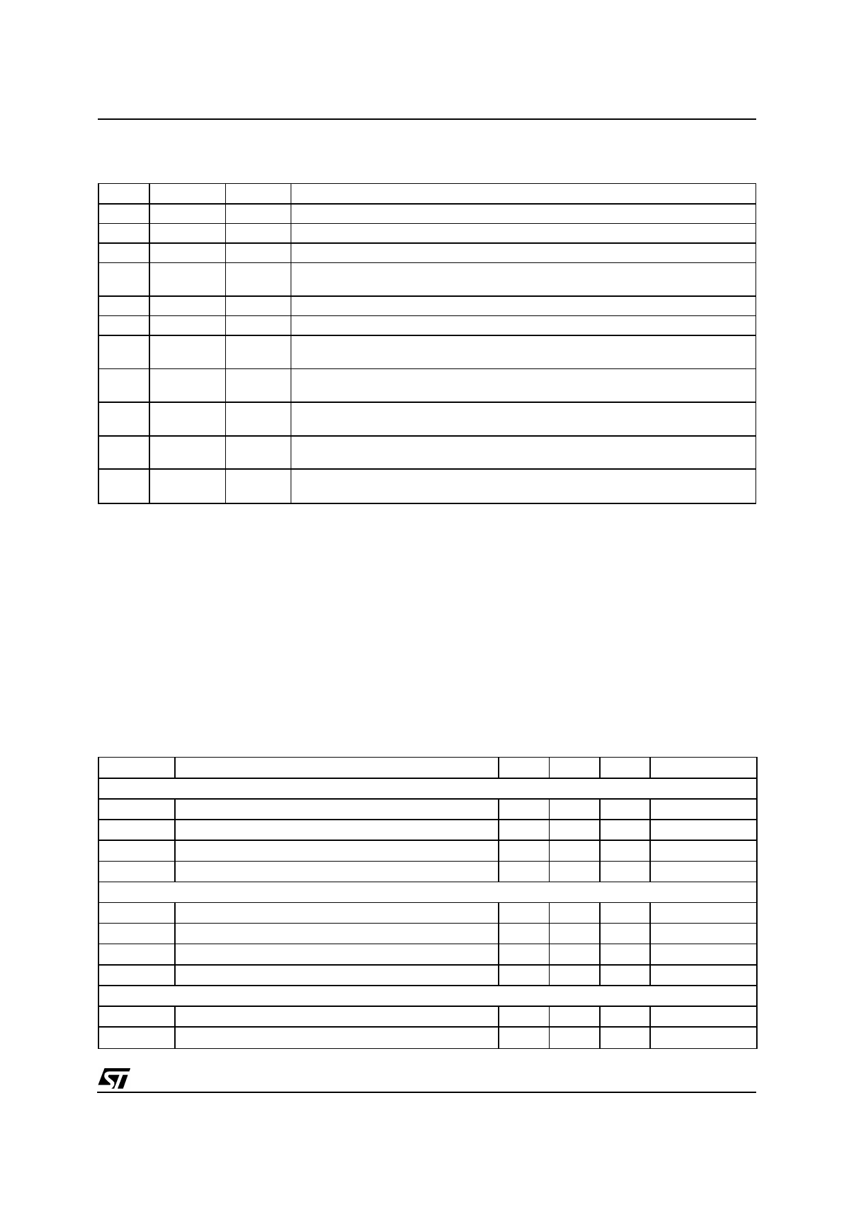
PIN FUNCTIONS (continued)
N.
Name
Type
Description
70
PGND
I
PLL Ground Input. Ground connection for Oscillator circuit
71
PVCC
I
PLL Power Supply Positive. Supply for PLL Clock Oscillator
72
XTO
O
Crystal Oscillator Output. Crystal Oscillator Output drive
73
ALE
O
EMI Address Latch Enable. This pin acts as the EMI Address Latch Enable for the
External Memory Interface. In DRAM mode acts as Column Address Strobe.
74
GND
I
Ground
75
DRDN
O
EMI Read Enable. This pin serves as the read enable for the EMI
76 EMI_AD0
I/O
EMI Multiplexed Address/Data Line 0. these pin acts as the EMI multiplexed
address and data line 0 In DRAM mode acts as Data 0.
77 EMI_AD1
I/O
EMI Multiplexed Address/Data Line 1. these pin acts as the EMI multiplexed
address and data line 1 In DRAM mode acts as Data 1.
78 EMI_AD2
I/O
EMI Multiplexed Address/Data Line 2. these pin acts as the EMI multiplexed
address and data line 2 In DRAM mode acts as Data 2.
79 EMI_AD3
I/O
EMI Multiplexed Address/Data Line 3. these pin acts as the EMI multiplexed
address and data line 3. In DRAM mode acts as Data 3.
80 EMI_AD4
I/O
EMI Multiplexed Address/Data Line 4. these pin acts as the EMI multiplexed
address and data line 4. In DRAM mode acts as Address 0.
All digital pins are TTL Schmitt Trigger, 5V tolerant.
POWER DISSIPATION
Power consumption depends on application run-
ning and DSP clock frequency.
Medium consumption running a typical applica-
tion like Echo and Noise cancellation:
DSP clock freq. = 43MHz
V = 3.3
Idd = 145mA
Ptot = 478mW
Max consumption with high stress test program:
DSP clock freq. = 43MHz
V = 3.3
Idd = 230mA
Ptot = 759mW
KEY PARAMETERS
Table 1.
Symbol
Parameter
GENERAL
fosc
Crystal frequency
Vdd
Operating voltage
IDD
Supply current
Tamb
Operating temperature
DSP CORE
fdsp
DSP clock frequency
Data bus width
Accumulator width
Multiplication unit
CODEC
SNR
Signal to noise ratio ADC
SNR
Signal to noise ratio DAC
Min. Typ. Max.
Unit
40
3.15 3.3
3.6
140 230
-40
85
MHz
V
mA
°C
45 48.2
24
56
24x24
MHz
bit
bit
bit
-70
dBr A weighted
-71
dBr A weighted
5/10
Share Link: 