IDT7MP4095S15Z View Datasheet(PDF) - Integrated Device Technology
Part Name
Description
Manufacturer
IDT7MP4095S15Z Datasheet PDF : 8 Pages
| |||
IDT7MP4060/7MP4095
128K x 32 CMOS STATIC RAM MODULES
COMMERCIAL TEMPERATURE RANGE
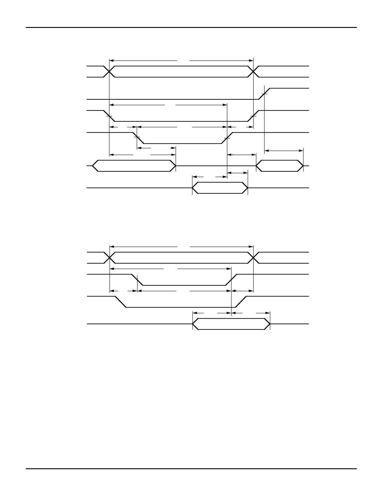
TIMING WAVEFORM OF WRITE CYCLE NO. 1 (WE CONTROLLED TIMING)(1, 2, 3, 7)
t WC
ADDRESS
OE
CS
WE
DATA OUT
DATA IN
t AW
t AS
t WP (7)
t WR
t WHZ (6)
t OHZ (6)
(4)
t OW (6)
t DH
t DW
DATA VALID
t OHZ (6)
(4)
3147 drw 07
TIMING WAVEFORM OF WRITE CYCLE NO. 2 (CS CONTROLLED TIMING)(1, 2, 3, 5)
ADDRESS
CS
WE
tAS
DATA IN
t WC
t AW
tCW
t WR
t DW
t DH
DATA VALID
3147 drw 08
NOTES:
1. WE or CS must be high during all address transitions.
2. A write occurs during the overlap (tWP) of a low CS and a low WE.
3. tWR is measured from the earlier of CS or WE going high to the end of write cycle.
4. During this period, I/O pins are in the output state, and input signals must not be applied.
5. If the CS low transition occurs simultaneously with or after the WE low transition, the outputs remain in a high impedance state.
6. Transition is measured ±200mV from steady state with a 5pF load (including scope and jig). This parameter is guaranteed by design, but not tested.
7. If OE is low during a WE controlled write cycle, the write pulse width must be the larger of tWP or (tWHZ + tDW).
7.09
6
Share Link: 