LC8903 View Datasheet(PDF) - SANYO -> Panasonic
Part Name
Description
Manufacturer
LC8903 Datasheet PDF : 15 Pages
| |||
LC8903, 8903Q
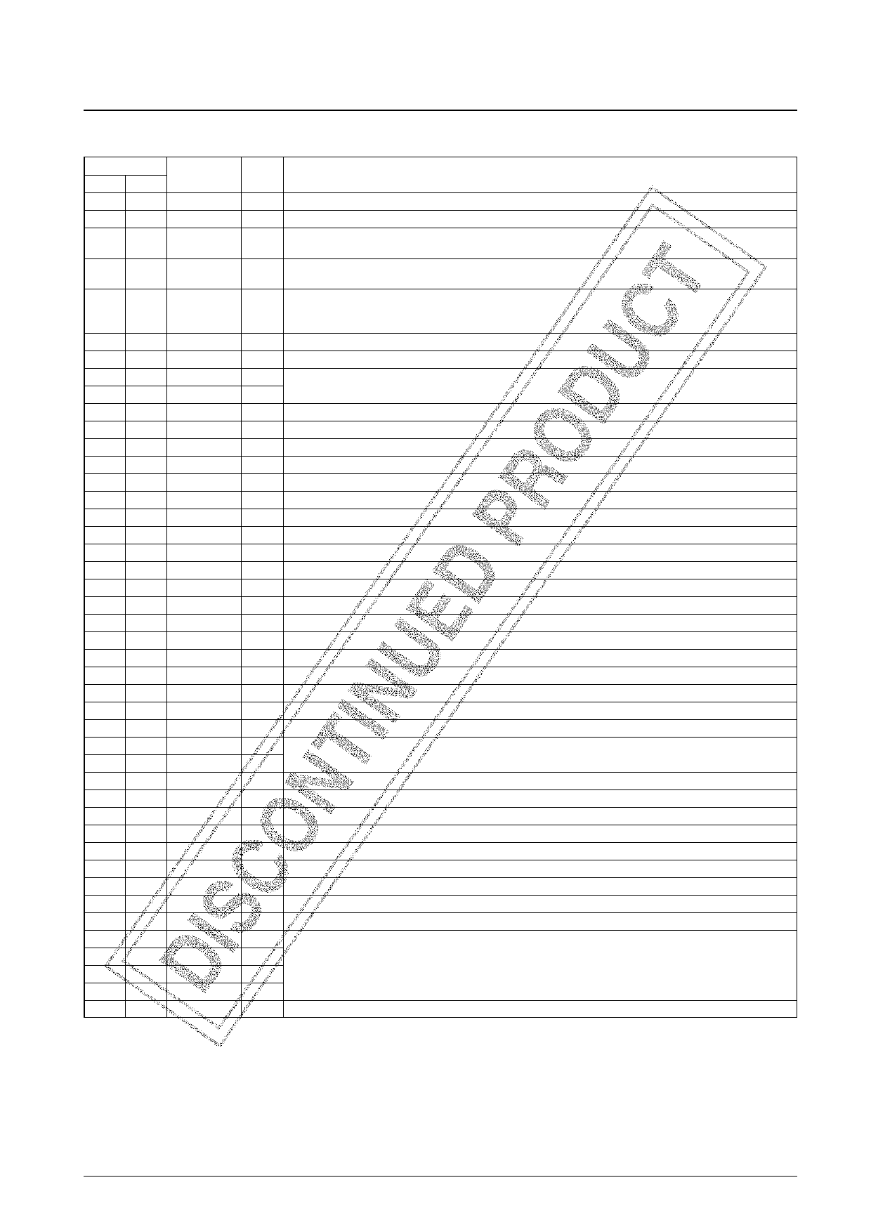
Pin Functions
Pin No.
QIP DIP
1
6
2
7
3
8
4
9
5
10
6
11
7
12
8
13
9
14
10
15
11
—
12
16
13
17
14
18
15
19
16
20
17
21
18
22
19
23
20
24
21
25
22
26
23
27
24
28
25
29
26
30
27
31
28
—
29
32
30
33
31
34
32
35
33
36
34
37
35
38
36
39
37
40
38
41
39
42
40
1
41
2
42
3
43
4
44
5
Symbol
DIN5
DOUT1
V/DOUT2
RC1
RC2
CLKMD
CLK
TEST1
TEST2
XMODE
DVDD
AVDD
R
AGND
VIN
VCO
DGND
SBSY
PW
SFSY
SBCK
DVDD
XIN
XOUT
CLK OUT1
CLK OUT2
ERROR
DGND
SUB1
SUB2
BCLK
DATA OUT
LRCK
EMPHA
DO
DI
CE
CL
DVDD
DIN1
DIN2
DIN3
DIN4
DGND
I/O
Function
I Data input. There is no built-in amplifier on this pin.
O EIAJ data through output
Validity flag output
O Alternatively, the microprocessor interface can set this pin to output the EIAJ input data unchanged.
RC oscillator input
I
This circuit generates a clock used to detect incorrect PLL locking and to reset the PLL system.
RC oscillator output
O This pin outputs a clock with a frequency of about 40 kHz when the component values specified in the sample
application circuit are used.
I CLKOUT2 output clock switching: Low = 256 fs, high = 128 fs
I Clock mode switching: Low = 384 fs, high = 512 fs
I
Test pin (Should be tied low in normal operation.)
I
I Used to start system operation after power is applied.
Digital power supply
Analog power supply
I VCO oscillator band adjustment
Analog ground
I VCO free-running setting
O PLL low-pass filter
Digital system ground
O Subcode interface block sync signal
O Subcode interface data output
O Subcode interface frame sync signal
I Subcode interface bit clock input
Digital power supply
I Crystal oscillator input
O Crystal oscillator output
O Crystal oscillator and VCO clock output
O 256 fs and 128 fs clock output
O Error mute signal output
Digital ground
O
Sampling frequency output
O
O Bit clock output
O Audio data output
O Left/right clock output
O High = emphasis on, low = emphasis off. Outputs a low level in analog mode.
O Microprocessor interface output
I Microprocessor interface input
I Microprocessor interface chip enable input
I Microprocessor interface clock input
Digital power supply
I
I
Data inputs with built-in amplifiers
I
I
Digital ground
No. 4542-7/15
Share Link: 