BD2062FJ_REV_A View Datasheet(PDF) - ROHM Semiconductor
Part Name
Description
Manufacturer
BD2062FJ_REV_A Datasheet PDF : 5 Pages
| |||
2/4
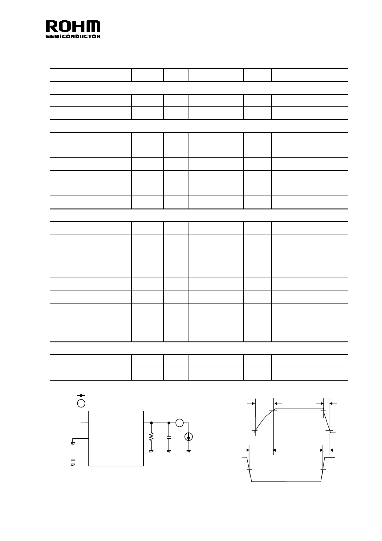
◇Electric characteristics
Unless otherwise specified VIN = 5.0V, Ta = 25°C
Parameter
Symbol Min.
Current consumption
Operating Current
Standby Current
IDD
-
ISTB
-
I/O
/EN input voltage
/EN input current
V/EN
V/EN
I/EN
2.0
-
-1.0
/OC output LOW voltage
/OC output leak current
V/OCL
-
IL/OC
-
/OC delay time
T/OC
10
Power switch
ON resistance
Current Limit Threshold
RON
-
ITH
1.5
Short-circuit current
ISC
1.1
Output rise time
Output rise delay time
Output fall time
Output fall delay time
Switch leak current
Reverse leak current
UVLO
UVLO
Threshold
◇Measurement circuit
VIN
A
TON1
-
TON2
-
TOFF1
-
TOFF2
-
ILSW
-
ILREV
-
VTUVH
2.1
VTUVL
2.0
V/EN
IN
GND
/EN
OUT
A
RL CL
/OC
Typ.
Max.
Unit
Condition
130
180
0.01
1
μA
V/EN = 0V, OUT = OPEN
μA
V/EN = 5V, OUT = OPEN
-
-
-
0.8
0.01
1.0
-
0.5
0.01
1
15
20
V
High input
V
Low input
μA
V/EN = 0V or 5V
V
I/OC = 0.5mA
μA
V/OC = 5V
ms
80
125
mΩ IOUT = 500mA
2.4
3.0
A
1.5
2.1
A
VOUT = 0V, CL = 47μF
RMS
0.8
10
ms
RL = 10Ω
1.1
20
ms
RL = 10Ω
5
20
μs
RL = 10Ω
10
40
μs
RL = 10Ω
-
1.0
μA
V/EN = 5V, VOUT = 0V
-
1.0
μA
VOUT = 5.5V, VIN = 0V
2.3
2.5
V
Increasing VIN
2.2
2.4
V
Decreasing VIN
◇Timing chart at output rise / fall time
VOUT
TON1
90%
TOFF1
90%
IOUT
10%
V/EN
TON2
10%
TOFF2
50%
50%
REV. A
Share Link: 