74OL6011SD View Datasheet(PDF) - Fairchild Semiconductor
Part Name
Description
Manufacturer
74OL6011SD Datasheet PDF : 15 Pages
| |||
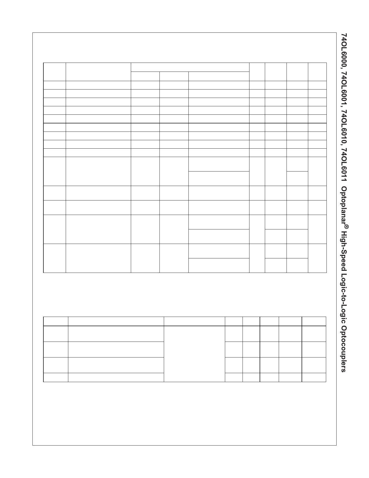
Electrical Characteristics (TA = 0┬░C to 70┬░C Unless otherwise speci№гЂed)
CMOS Output 74OL6010 and 74OL6011(3)
Test Conditions
Symbol
Parameter
74OL6010 74OL6011
74OL6010/11
VCCI
VCCO
VIH
VIL
VIK
IIH
IIL
ICCIH
ICCIL
VOL
Input Supply Voltage
Output Supply Voltage(4)
High-Level Input Voltage
Low-Level Input Voltage
Input Clamp Voltage
High-Level Input Current
Low-Level Input Current
Input Supply Current (HIGH)
Input Supply Current (LOW)
Low-Level Output Voltage VIN = 0.8V
IOH High-Level Output Current VIN = VIH
IOL Low-Level Output Current VIN = 0.8V
ICCOH Output Supply Current
(HIGH)
VIN = VIH
ICCOL Output Supply Current
(LOW)
VIN = VIL
*All typical values are at TA=25┬░C
VIN = 2.0V
VIN = VIL
VIN = 2.0V
VIN = VIL
VIN = VIH
VCCI = 4.5V, II = -18mA
VCCI = 5.5V, VIH = 4.5V
VCCI = 5.5V, VIL = -0.4V
VCCI = 5.5V, VIN = VIH
VCCI = 5.5V, VIN = VIL
VCCI = 4.5V, VCCO = 4.5V,
IOL = 16mA
VCCI = 4.5V, VCCO = 4.5V,
IOL = 4mA
VCCI = 4.5V, VOH = 15V,
VCCO = 4.5РђЊ15V
VCCI = 4.5V, VOL = 0.6V,
VCCO = 4.5РђЊ15V
VCCI = 5.5V, VO = VOH,
VCCO = 4.5V
VCCI = 5.5V, VO = VOL,
VCCO = 15V
VCCI = 5.5V, VO = VOL,
VCCO = 4.5V
VCCI = 5.5V, VO = VOL,
VCCO = 15V
Min.
4.5
4.5
2.0
Typ.*
5.0
1.0
-200.0
10.0
10.0
0.4
1.0
16.0
9.0
11.0
8.0
11.0
Max.
5.5
15.0
0.8
-1.2
40.0
-400.0
14.0
14.0
0.6
Units
V
V
V
V
V
┬хA
┬хA
mA
mA
V
0.5
100.0 ┬хA
mA
12.0 mA
18.0
12.0 mA
18.0
Switching Characteristics (TA = 25┬░C Unless otherwise speci№гЂed)
TTL Output 74OL6010 and 74OL6011(3)
Symbol
Parameter
Test Conditions Min. Typ. Max.
tPHL Propagation Delay Time For Output
Low Level
tPLH Propagation Delay Time For Output
High Level
VCCI = 5V, VCCO = 5V,
RL = 470Рёд
60 120
100 180
tr Output Rise Time For Output High
50
Level
tf Output Fail Time For Output Low Level
5
Units
ns
ns
ns
ns
Fig.
15, 18
15, 18
15, 18
15, 18
Notes:
3. The VCCO and VCCI supply voltages to the device must each be bypassed by a 0.1┬хF capacitor or larger. This can
be either a ceramic or solid tantalum capacitor with good high frequency characteristics. Its purpose is to stabilize
the operation of the high-gain amplifiers. Failure to provide the bypass will impair the DC and switching properties.
The total lead length between capacitor and optocoupler should not exceed 1.5mm. See Fig. 20.
4. For example, assuming a VCCI of 5.0V, and an ambient temperature of 70┬░C, the maximum allowable VCCO is 12.1V.
┬Е2000 Fairchild Semiconductor Corporation
74OL60XX Rev. 1.0.4
6
www.fairchildsemi.com
Share Link: 