FDG328P View Datasheet(PDF) - TY Semiconductor
Part Name
Description
Manufacturer
FDG328P Datasheet PDF : 2 Pages
| |||
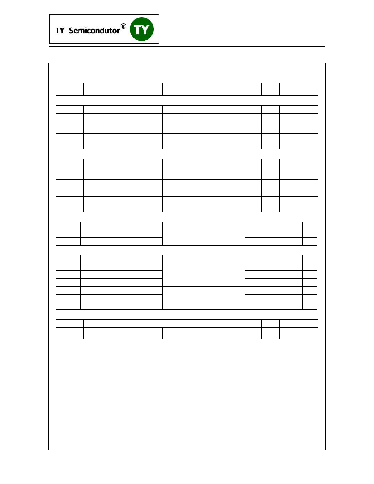
Product specification
FDG328P
Electrical Characteristics
Symbol
Parameter
TA = 25°C unless otherwise noted
Test Conditions
Min Typ Max Units
Off Characteristics
BVDSS
Drain–Source Breakdown Voltage VGS = 0 V, ID = –250 µA
–20
V
∆BVDSS
∆TJ
IDSS
Breakdown Voltage Temperature
Coefficient
Zero Gate Voltage Drain Current
ID = –250 µA, Referenced to 25°C
VDS = –16 V, VGS = 0 V
–9
mV/°C
–1
µA
IGSSF
Gate–Body Leakage, Forward
VGS = 12 V, VDS = 0 V
100 nA
IGSSR
Gate–Body Leakage, Reverse
VGS = –12 V, VDS = 0 V
–100 nA
On Characteristics (Note 2)
VGS(th)
Gate Threshold Voltage
∆VGS(th)
∆TJ
RDS(on)
Gate Threshold Voltage
Temperature Coefficient
Static Drain–Source
On–Resistance
ID(on)
On–State Drain Current
gFS
Forward Transconductance
VDS = VGS, ID = –250 µA
–0.6
–1.5
V
ID = –250 µA, Referenced to 25°C
3
mV/°C
VGS = –4.5 V, ID = –1.5 A
120 145 mΩ
VGS = –2.5 V, ID = –1.2 A
169 210
VGS = –4.5 V, ID = –1.5 A, TJ=125°C
156 203
VGS = –4.5 V, VDS = –5 V
–3
A
VDS = –5 V,
ID = –1.5 A
5
S
Dynamic Characteristics
Ciss
Input Capacitance
Coss
Output Capacitance
Crss
Reverse Transfer Capacitance
VDS = –10 V, V GS = 0 V,
f = 1.0 MHz
Switching Characteristics
td(on)
Turn–On Delay Time
tr
Turn–On Rise Time
td(off)
Turn–Off Delay Time
tf
Turn–Off Fall Time
Qg
Total Gate Charge
Qgs
Gate–Source Charge
Qgd
Gate–Drain Charge
(Note 2)
VDD = –10 V, ID = 1 A,
VGS = –4.5 V, RGEN = 6 Ω
VDS = –10 V, ID = –1.5 A,
VGS = –4.5 V
Drain–Source Diode Characteristics and Maximum Ratings
IS
Maximum Continuous Drain–Source Diode Forward Current
VSD
Drain–Source Diode Forward
VGS = 0 V, IS = –0.62 A (Note 2)
Voltage
337
pF
88
pF
51
pF
9
18 ns
12 22 ns
10 20 ns
5
10 ns
3.7
6 nC
0.7
nC
1.3
nC
–0.62 A
–0.7 –1.2
V
Notes:
1. RθJA is the sum of the junction-to-case and case-to-ambient thermal resistance where the case thermal reference is defined as the solder mounting surface of
the drain pins. RθJC is guaranteed by design while RθCA is determined by the user's board design.
a.) 170°/W when mounted on a 1 in2 pad of 2 oz. copper.
b.) 260°/W when mounted on a minimum pad.
2. Pulse Test: Pulse Width < 300µs, Duty Cycle < 2.0%
http://www.twtysemi.com
sales@twtysemi.com
4008-318-123
2 of 2
Share Link: 