74ABT16240ADGG View Datasheet(PDF) - Philips Electronics
Part Name
Description
Manufacturer
74ABT16240ADGG Datasheet PDF : 10 Pages
| |||
Philips Semiconductors
16-bit inverting buffer/driver (3-State)
Product specification
74ABT16240A
74ABTH16240A
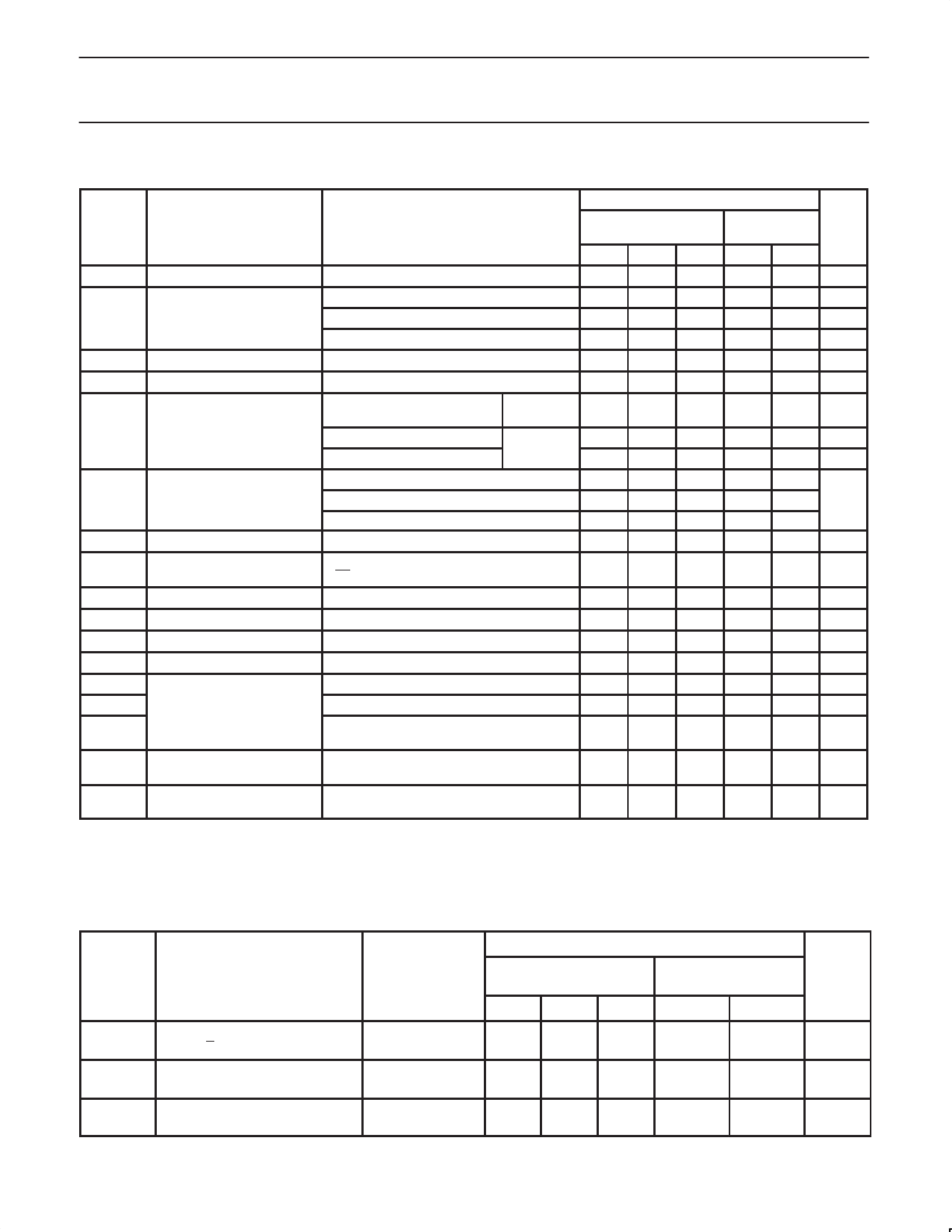
DC ELECTRICAL CHARACTERISTICS
LIMITS
SYMBOL
PARAMETER
TEST CONDITIONS
Tamb = +25°C
Tamb = –40°C
to +85°C
Min Typ Max Min Max
VIK
Input clamp voltage
VCC = 4.5V; IIK = –18mA
–0.9 –1.2
–1.2
VCC = 4.5V; IOH = –3mA; VI = VIL or VIH
2.5 2.9
2.5
VOH High-level output voltage
VCC = 5.0V; IOH = –3mA; VI = VIL or VIH
3.0 3.4
3.0
VCC = 4.5V; IOH = –32mA; VI = VIL or VIH
2.0 2.4
2.0
VOL Low-level output voltage
VCC = 4.5V; IOL = 64mA; VI = VIL or VIH
0.42 0.55
0.55
II
Input leakage current
VCC = 5.5V; VI = GND or 5.5V
±0.01 ±1.0
±1.0
II
Input leakage current
74ABTH16240A
VCC = 5.5V; VI = VCC or GND
VCC = 5.5V; VI = VCC
Control
pins
Data pins
±0.01 ±1
0.01
1
±1
1
VCC = 5.5V; VI = 0
–2
–3
–5
IHOLD
Bus Hold current A inputs
74ABTH16240A3
VCC = 4.5V; VI = 0.8V
VCC = 4.5V; VI = 2.0V
50
50
–75
–75
VCC = 5.5V; VI = 0 to 5.5V
±500
IOFF Power-off leakage current
VCC = 0.0V; VO or VI ≤ 4.5V
±5.0 ±100
±100
IPU/IPD
Power-up/down 3-State
output current
VCC = 2.0V; VO = 0.5V; VI = GND or VCC;
VOE = VCC
±5.0 ±50
±50
IOZH 3-State output High current VCC = 5.5V; VO = 2.7V; VI = VIL or VIH
1.0
10
10
IOZL 3-State output Low current
VCC = 5.5V; VO = 0.5V; VI = VIL or VIH
–1.0 –10
–10
ICEX Output high leakage current VCC = 5.5V; VO = 5.5V; VI = GND or VCC
1.0
50
50
IO
Output current1
VCC = 5.5V; VO = 2.5V
–50 –70 –180 –50 –180
ICCH
VCC = 5.5V; Outputs High, VI = GND or VCC
0.5 1.0
1.0
ICCL Quiescent supply current
VCC = 5.5V; Outputs Low, VI = GND or VCC
8
19
19
ICCZ
VCC = 5.5V; Outputs 3-State;
VI = GND or VCC
0.5 1.0
1.0
∆ICC
Additional supply current per Outputs enabled, one input at 3.4V, other
input pin2 74ABT16240A
inputs at VCC or GND; VCC = 5.5V
10 200
200
∆ICC
Additional supply current per Outputs enabled, one input at 3.4V, other
input pin2 74ABTH16240A
inputs at VCC or GND; VCC = 5.5V
0.2 1.0
1.0
NOTES:
1. Not more than one output should be tested at a time, and the duration of the test should not exceed one second.
2. This is the increase in supply current for each input at 3.4V.
3. This is the bus hold overdrive current required to force the input to the opposite logic state.
UNIT
V
V
V
V
V
µA
µA
µA
µA
µA
µA
µA
µA
µA
µA
mA
mA
mA
mA
µA
mA
AC CHARACTERISTICS
GND = 0V; tR = tF = 2.5ns; CL = 50pF; RL = 500Ω; Tamb = -40°C to +85°C.
LIMITS
SYMBOL
PARAMETER
WAVEFORM
Tamb = +25°C
VCC = +5.0V
Min
Typ
Max
Tamb = –40°C to +85°C
VCC = +5.0V ±0.5V
Min
Max
tPLH
Propagation delay
tPHL
nAx to nYx
tPZH
Output enable time
tPZL
to High and Low level
tPHZ
Output disable time
tPLZ
from High and Low level
1
1.0
2.0
3.0
1.0
3.7
1.0
1.5
3.0
1.0
3.5
2
1.2
2.4
3.3
1.2
4.2
1.2
2.3
3.2
1.0
4.2
2
1.3
2.7
4.1
1.6
4.7
1.3
2.5
3.6
1.4
4.1
UNIT
ns
ns
ns
1998 Feb 25
5
Share Link: 