CXA7000R View Datasheet(PDF) - Sony Semiconductor
Part Name
Description
Manufacturer
CXA7000R Datasheet PDF : 23 Pages
| |||
CXA7000R
Pin Description
Pin
No.
Symbol
I/O
Standard
voltage level
1 FRP
I
High: ≥2.0V
Low: ≤0.8V
2 SHST
I
High: ≥2.0V
Low: ≤0.8V
3 POSCNT0
4
5
POSCNT1
POSCNT2
I
High: ≥2.0V
Low: ≤0.8V
6 POSCNT3
11 SIG.C
I 1 to 5.0V
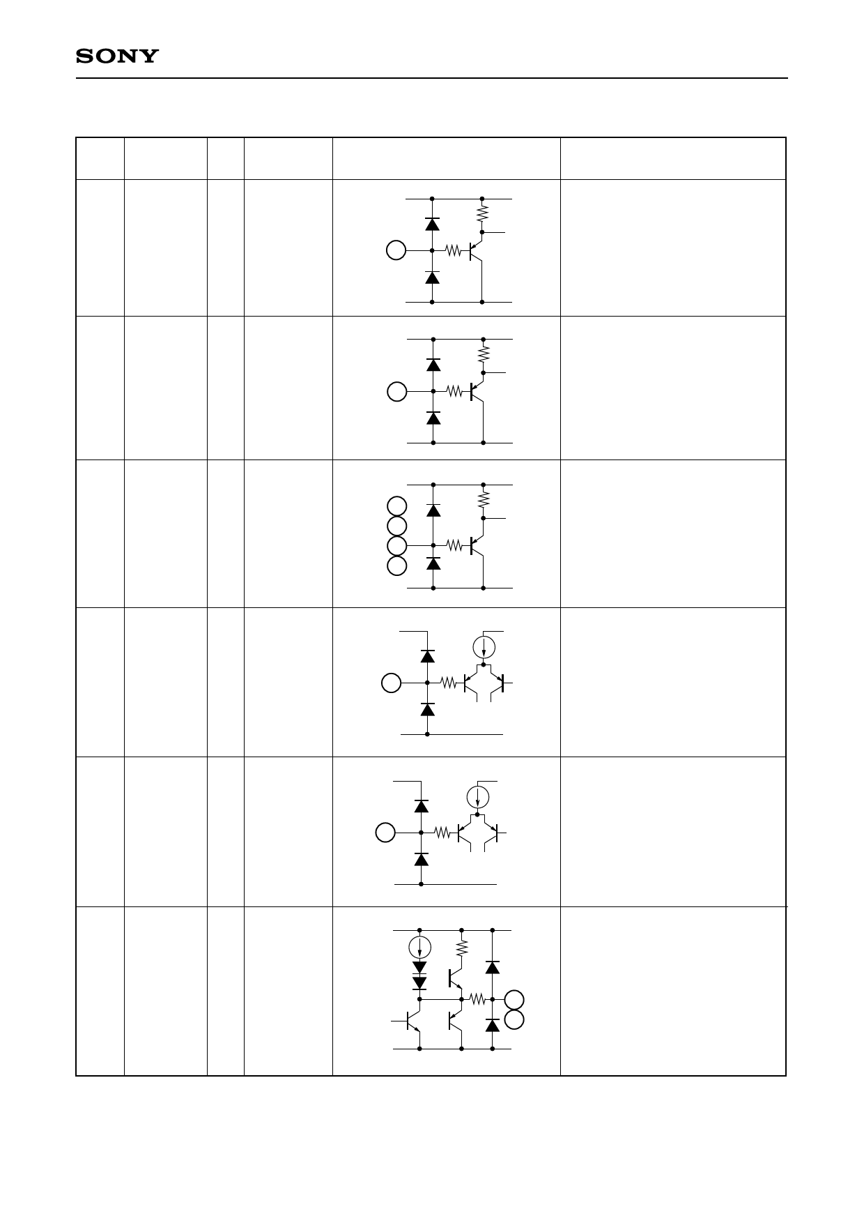
Equivalent circuit
VDD
50k
192
1
GND
VDD
2
50k
192
GND
VDD
3
4
5
6
GND
50k
192
VDD
30k
11
VCC
20µ
12 SIG_OFST I 0 to 5.0V
GND
VDD
30k
12
VCC
10µ
GND
VCC
13 CAL_L
14 CAL_H
I/O
3.0 to 6.0V
9.0 to 12.0V
GND
40µ 1k
145
13
14
Description
LCD panel AC drive inversion
timing input.
High: inverted
Low: non-inverted
See the Timing Chart.
Internal sample-and-hold timing
circuit reset pulse input.
This pin is also used as the
offset cancel level insertion
timing input.
A reset is applied to the internal
timing generator at the falling
edge.
Output phase adjustment.
The output phase is adjusted in
MCLK period units when
SL_DAT is high, and in
1/2 MCLK period units when
SL_DAT is low.
Signal center voltage (inversion
folded voltage) adjustment input.
The SH_OUT output center
voltage can be adjusted in the
range from 7.0 to 8.0V.
Output signal offset adjustment
from signal center voltage.
The SH_OUT output 100%
white level (at 3FF input) voltage
can be adjusted in the range
from 0 to 1V from the center
voltage.
Level output for canceling the
offset between channels.
Connect the CAL_L and
CAL_H, between ICs when
using two CXA7000R.
–3–
Share Link: 