LC75817NW View Datasheet(PDF) - SANYO -> Panasonic
Part Name
Description
Manufacturer
LC75817NW
SANYO -> Panasonic

LC75817NW Datasheet PDF : 43 Pages
| |||
LC75817NE, 75817NW
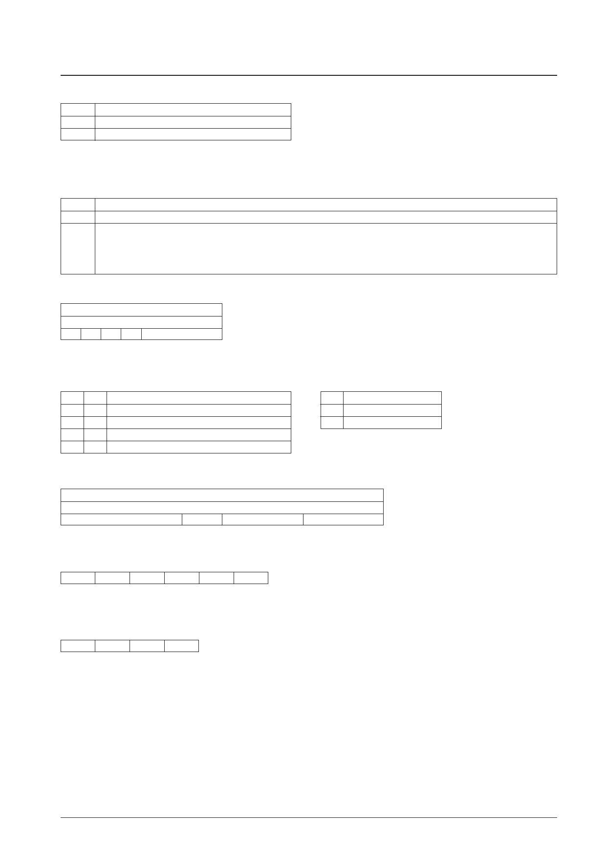
SC: Controls the common and segment output pins
SC
Common and segment output pin states
0 Output of LCD drive waveforms
1
Fixed at the VLCD4 level (all segments off)
Note: *13. When SC is 1, the S1 to S60 and COM1 to COM10 output pins are set to the VLCD4 level, regardless of the M, A, and DG1 to DG12 data.
SP: Controls the normal mode and sleep mode
SP
Mode
0 Normal mode
Sleep mode
The common and segment pins go to the VLCD4 level and the oscillator on the OSCI, OSCO pins is stopped (although it operates during key
1 scan operations) to reduce current drain. Although the “display on/off control”, “set display contrast”, “set key scan output state”, and “set
general-purpose output port state” instructions can be executed in this mode, applications must return the IC to normal mode to execute any of
the other instruction settings.
• Display shift ... <Shifts the display>
Code
D56 D57 D58 D59 D60 D61 D62 D63
M A R/L X 0 0 1 1
X: don’t care
M, A: Specifies the data to be shifted
MA
Shift operating state
0
0 Neither MDATA nor ADATA is shifted
0
1 Only ADATA is shifted
1
0 Only MDATA is shifted
1
1 Both MDATA and ADATA are shifted
R/L: Specifies the shift direction
R/L
Shift direction
0
Shift left
1
Shift right
• Set AC address... <Specifies the DCRAM and ADRAM address for AC>
Code
D48 D49 D50 D51 D52 D53 D54 D55 D56 D57 D58 D59 D60 D61 D62 D63
DA0 DA1 DA2 DA3 DA4 DA5 X X RA0 RA1 RA2 RA3 0 1 0 0
X: don’t care
DA0 to DA5: DCRAM address
DA0
DA1
DA2
DA3
LSB
↑
Least significant bit
RA0 to RA3: ADRAM address
DA4
DA5
MSB
↑
Most significant bit
RA0
RA1
LSB
↑
Least significant bit
RA2
RA3
MSB
↑
Most significant bit
This instruction loads the 6-bit DCRAM address DA0 to DA5 and the 4-bit ADRAM address RA0 to RA3 into the AC.
No. 6144-13/43
Share Link: