LC75817NW View Datasheet(PDF) - SANYO -> Panasonic
Part Name
Description
Manufacturer
LC75817NW
SANYO -> Panasonic

LC75817NW Datasheet PDF : 43 Pages
| |||
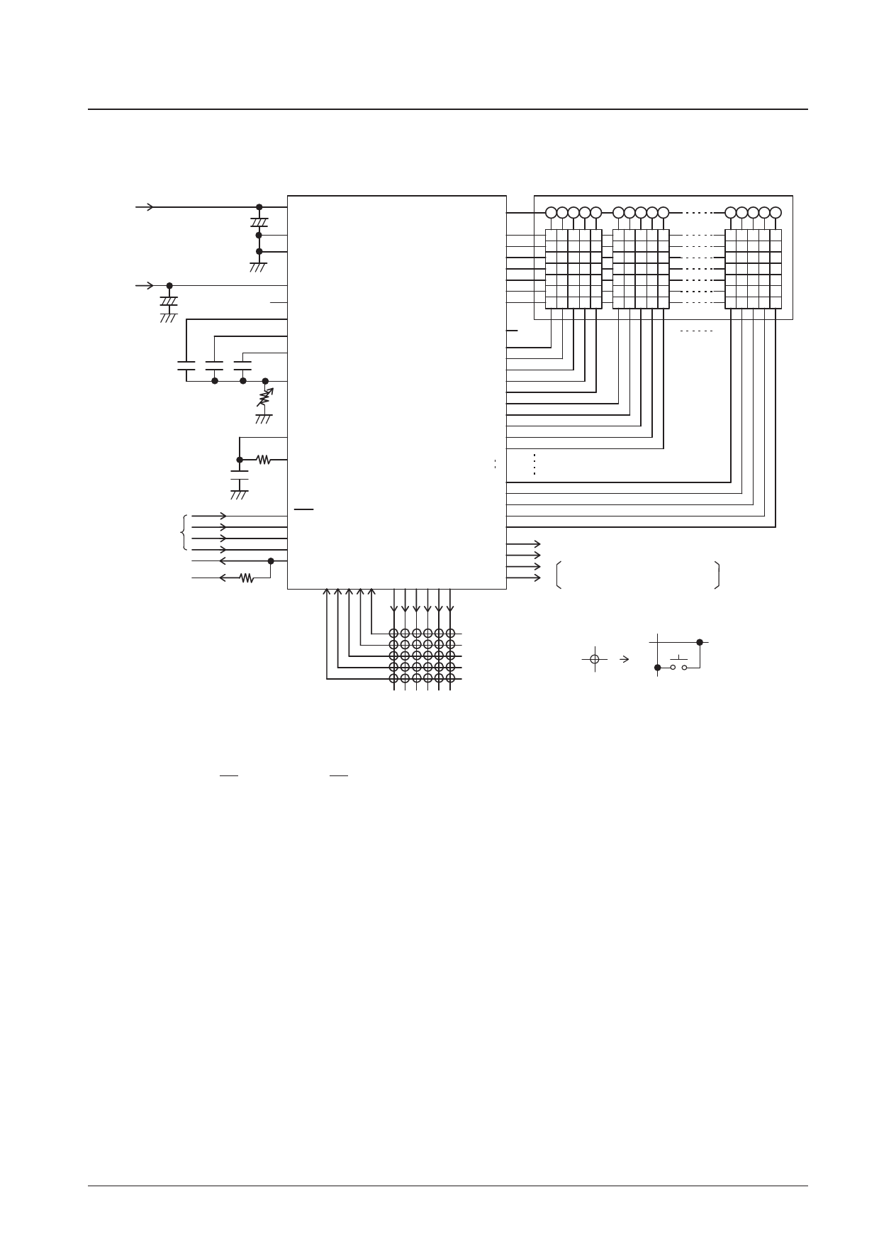
LC75817NE, 75817NW
Sample Application Circuit 1
1/8 duty, 1/4 bias drive technique (for use with normal panels)
+5V
*22
+8V
OPEN
CCC
C ≥ 0.047 µF
From the
controller
To the
controller
To the
controller
*25
power supply
LCD panel
VDD
TEST
VSS
VLCD
VLCD0
VLCD1
VLCD2
VLCD3
VLCD4 *23
OSCI
OSCO
COM1
COM2
COM3
COM4
COM5
COM6
COM7
COM8
COM9
S1
S2
S3
S4
S5
S6
S7
S8
S9
S10
OPEN
INH *24
CE
CL
DI K K K K K
DO I I I I I
54321
S56
S57
S58
S59
COM10/S60
KKKKKK
SSSSSS
P1
P2
P3
654321
P4
(general-purpose output ports)
used with the backlight controller
or other circuit
Key matrix
(up to 30 keys)
Notes: *22. Add a capacitor to the logic block power supply line so that the logic block power supply voltage VDD rise time when power is applied and the
logic block power supply voltage VDD fall time when power drops are both at least 1 ms, as the LC75817NE/NW is reset by the VDET.
*23. If a variable resistor is not used for display contrast fine adjustment, the VLCD4 pin must be connected to ground.
*24. If the function of INH pin is not used, the INH pin must be connected to the logic block power supply VDD.
*25. The DO pin, being an open-drain output, requires a pull-up resistor. Select a resistance (between 1 to 10 kΩ) appropriate for the capacitance of
the external wiring so that signal waveforms are not degraded.
No. 6144-31/43
Share Link: