GS841E18AB-100 View Datasheet(PDF) - Giga Semiconductor
Part Name
Description
Manufacturer
GS841E18AB-100 Datasheet PDF : 21 Pages
| |||
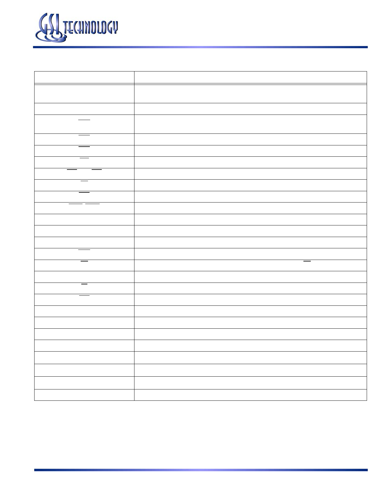
TQFP Pin Description
Symbol
An
CLK
BWE
BW1
BW2
GW
CE1,CE2, CE3
OE
ADV
ADSP, ADSC
DQ
DQP
MATCH
MOE
DE
ZZ
FT
LBO
TMS
TDI
TDO
TCK
VDD
VSS
VDDQ
NC
GS841E18AT/B-180/166/150/130/100
Description
Address Input Signals—Inputs are registered and must meet setup and hold times, as specified on
page 11.
Clock Input Signal
Byte Write Enable Signal—The byte write enable signal needs to be combined with one of the four
byte write signals for a write operation to occur.
Byte Write signal for data outputs 1 thru 8
Byte Write signal for data outputs 9 thru 16
Global Write Enable
Chip Enables
Output Enable
Burst address advance
Address status signals
Data Input and Output pins
Parity Input and Output pins
Match Output
Match Output Enable
Data Enable—Data input registers are updated only when DE is active.
Power down control—Application of ZZ will result in a low standby power consumption.
Flow Through or Pipeline mode
Linear Order Burst mode
Test Mode Select
Test Data In
Test Data Out
Test Clock
3.3 V power supply
Ground
2.5 V/3.3 V output power supply
No Connect
Rev: 1.03 4/2005
4/21
Specifications cited are subject to change without notice. For latest documentation see http://www.gsitechnology.com.
© 2001, GSI Technology
Share Link: 